Improved rapid thinning method of gallium arsenide substrate

A gallium arsenide and substrate technology, applied in the manufacturing of electrical components, circuits, semiconductor/solid-state devices, etc., can solve the problems of GaAs metal pollution, easy introduction of pollutants, performance loss, etc.

Active Publication Date: 2012-07-04
INST OF MICROELECTRONICS CHINESE ACAD OF SCI
View PDF5 Cites 16 Cited by
  • Summary
  • Abstract
  • Description
  • Claims
  • Application Information

AI Technical Summary

Problems solved by technology

For example, when the Mohs hardness is greater than 4, the thinning of the gallium arsenide wafer will easily cause the accumulation of surface stress to form wafer curling. The direct consequence is that the change of the epitaxial layer

Method used


Image

  • Improved rapid thinning method of gallium arsenide substrate
  • Improved rapid thinning method of gallium arsenide substrate
  • Improved rapid thinning method of gallium arsenide substrate

Examples


Embodiment Construction

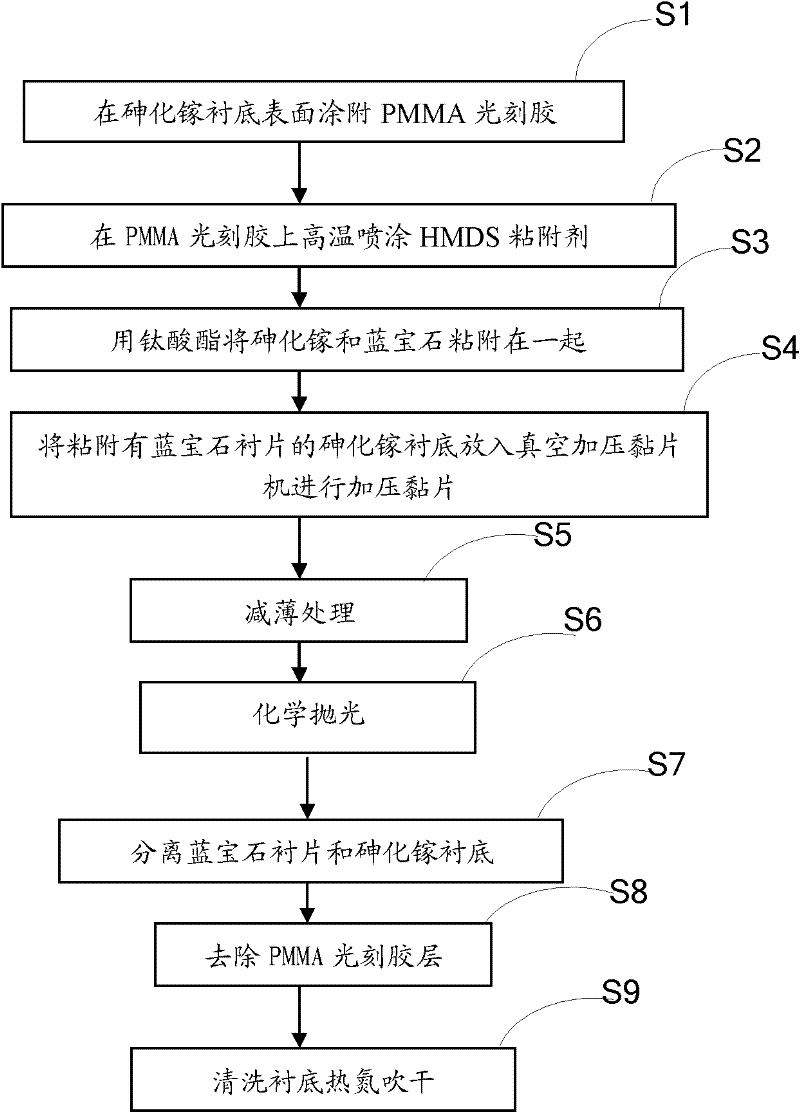
[0025] Such as figure 1 As shown, the technical process provided by the embodiment of the present invention specifically follows the steps:

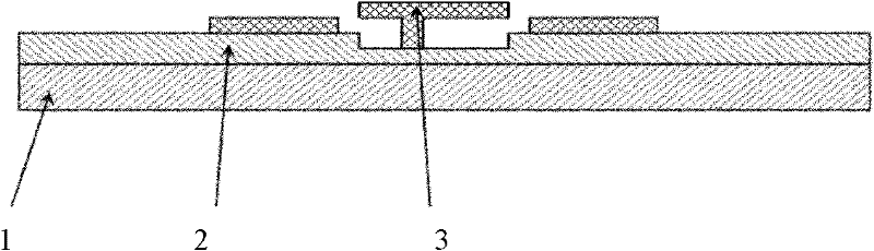
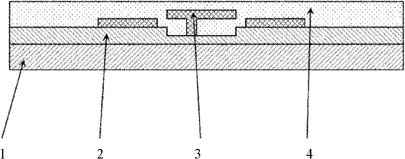
[0026] Step S1, the gallium arsenide substrate 1 with epitaxial layer 2 and circuit metal 3 (see figure 2 ) is coated with a PMMA (polymethyl methacrylate) photoresist layer 4 (see image 3 ),stand-by;

[0027] Step S2, spraying the HMDS (hexamethyldisilamine) 5 adhesive on the PMMA photoresist layer 4 at a high temperature of 120 to 150°C (actually, 90°C, 120°C, 135°C can also be selected) (see Figure 4 ), the thickness of the HMDS layer formed by spraying the HMDS adhesive on the PMMA photoresist layer is 0.1-1 μm (for example, 0.5 μm, 0.8 μm).

[0028] Step S3, place the gallium arsenide substrate adhered with HMDS on a hot plate at 130-150°C (for example, 120°C, 140°C) and pass titanate adhesive 6 (see Figure 5 ) attach the sapphire backing 7 to it (see Figure 6 ), the titanate adhesive is a titanate adhesive whose main comp...


PUM

PropertyMeasurementUnit
Thicknessaaaaaaaaaa

Abstract

The invention discloses an improved rapid thinning method of a gallium arsenide substrate. The method comprises the following steps of: based on the gallium arsenide substrate, carrying out adhesion on a gallium arsenide epitaxial wafer through a chemical reagent; meanwhile, utilizing a vacuum pressurizing method to fix, and utilizing a multilayer stacking structure to buffer the loss caused by thinning and reduce size distortion; and utilizing a soft ceramic grinding disc made of a unique material to realize high-speed and accurate back thinning, and cooperatively utilizing mixed aluminum oxide grinding slurry to obtain the thickness which is less than 60 mu m. After the grinding process is finished, a nano polishing solution is used for carrying out a CMP (Chemically Mechanical Polishing) process to achieve high-mirror effects that the thickness of a substrate is less than 50 mu m, the tolerance is less than +/-1 mu m and the roughness Ra is less than 1 nm. The polished substrate has the effects of no cracking, no crimping, no scratches and the like.

Description

technical field [0001] The invention relates to the technical field of semiconductors, in particular to an improved rapid thinning method of a gallium arsenide substrate. Background technique [0002] Gallium arsenide (GaAs) is one of the most important and widely used materials in III-V compound semiconductors. It has a large band gap, high electron mobility, small dielectric constant, and can introduce deep-level impurities, electrons The effective mass is small, the energy band structure is special, and it has a dual-energy valley conduction band. It can be used to prepare light-emitting devices, semiconductor lasers, microwave body effect devices, solar cells and high-speed integrated circuits. It is widely used in radars, electronic computers, artificial satellites, and spacecraft. and other cutting-edge technologies. GaAs has some better electronic properties than Si, such as high saturation electron velocity and high electron mobility, so that GaAs can be used in app...

Claims


Application Information

Patent Timeline
IPC IPC(8): H01L21/02
Inventor 汪宁陈中子陈晓娟刘新宇罗卫军庞磊
Owner INST OF MICROELECTRONICS CHINESE ACAD OF SCI
Why Eureka
Try Eureka