Supercharge Your Innovation With Domain-Expert AI Agents!

Silicon two-way transient voltage suppression diode and manufacture method thereof

A technology of transient voltage suppression and manufacturing method, which is applied in semiconductor/solid-state device manufacturing, circuits, electrical components, etc., to achieve the effects of good reliability, small size, and large instantaneous power absorption

Active Publication Date: 2015-03-04
CHINA ZHENHUA GRP YONGGUANG ELECTRONICS CO LTD STATE OWNED NO 873 FACTORY
View PDF6 Cites 0 Cited by
  • Summary
  • Abstract
  • Description
  • Claims
  • Application Information

AI Technical Summary

Problems solved by technology

In recent years, electronic components used in aviation and aerospace have been developing toward miniaturization. The original metal package and glass passivation package transient voltage suppression diodes can no longer meet the requirements. Smaller transient voltage suppression diodes are required to meet the requirements. Requirements for miniaturization of electronic equipment

Method used


Image

  • Silicon two-way transient voltage suppression diode and manufacture method thereof
  • Silicon two-way transient voltage suppression diode and manufacture method thereof
  • Silicon two-way transient voltage suppression diode and manufacture method thereof

Examples


Embodiment Construction

[0018] The present invention will be further described in detail below in conjunction with the accompanying drawings and embodiments, but not as any limitation to the present invention.

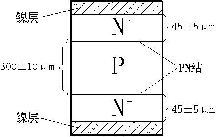
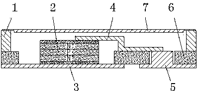
[0019] Embodiments of the present invention: a method of manufacturing a silicon bidirectional transient voltage suppressor diode of the present invention is to diffuse two N regions on both sides of a P-type silicon chip, plate nickel on the surface of the two N regions, and obtain positive hexagons after slicing. Form the chip, package the chip in the tube shell, and lead out the electrode to obtain a silicon bidirectional transient voltage suppression diode. The diffusion uses a diffusion mesa process for phosphorus diffusion. The P-type silicon wafer is a P-type dislocation-free silicon single wafer, the resistivity is between 0.09-0.15Ω.cm, and the thickness is between 290-310 μm. The thickness of the N region is between 40-50 μm. The surface of the N region is nickel-plated after ...


PUM


Abstract

The invention discloses a silicon two-way transient voltage suppression diode and a manufacture method thereof. The manufacture method comprises the steps of: diffusing to form two N regions on two surfaces of a P type silicon chip, plating nickel on the surfaces of the two N regions, and obtaining an orthohexagnal chip after scribing; and encapsulating the orthohexagnal chip into a diode housing, and extracting an electrode to obtain the silicon two-way transient voltage suppression diode. The silicon two-way transient voltage suppression diode is encapsulated by adopting a surface mounting device manner, and has the characteristics of small volume, light weight, large transient absorbed power and high reliability. Along with an weaponry system developed in minimization and intelligentization directions, a surface mounting type transient voltage suppression diode with smaller volume and more convenience for installation has a better development prospect; and meanwhile, a very advanced parallel seal welding encapsulation technology is adopted in a development process, so that an internal atmosphere of the silicon two-way transient voltage suppression diode can be controlled to be in a lower level, and the service life of the silicon two-way transient voltage suppression diode can be prolonged. The silicon two-way transient voltage suppression diode has better reliability.

Description

technical field [0001] The invention relates to a silicon bidirectional transient voltage suppression diode and a manufacturing method, belonging to the technical field of semiconductor diode manufacturing. Background technique [0002] A transient voltage suppressor diode is a high-performance circuit protection device. In recent years, electronic components used in aviation and aerospace have been developing toward miniaturization. The original metal package and glass passivation package transient voltage suppression diodes can no longer meet the requirements. Smaller transient voltage suppression diodes are required to meet the requirements. Requirements for miniaturization of electronic equipment. Contents of the invention [0003] The object of the present invention is to provide a silicon bidirectional transient voltage suppressor diode and its manufacturing method, so as to reduce the volume of the silicon bidirectional transient voltage suppressor diode and facili...

Claims


Application Information

Patent Timeline
Patent Type & Authority Patents(China)
IPC IPC(8): H01L21/329H01L21/60H01L21/22H01L23/485
CPCH01L24/34H01L2224/40225H01L2924/00014H01L24/40H01L2224/37099
Inventor 周鹏吴贵松周廷荣
Owner CHINA ZHENHUA GRP YONGGUANG ELECTRONICS CO LTD STATE OWNED NO 873 FACTORY
Features
  • R&D
  • Intellectual Property
  • Life Sciences
  • Materials
  • Tech Scout
  • Unparalleled Data Quality
  • Higher Quality Content
  • 60% Fewer Hallucinations
Learn More