Columnar bump packaging process

A packaging process and columnar bump technology, which is used in the manufacture of electrical components, electric solid-state devices, semiconductor/solid-state devices, etc., can solve the problems of short circuit of solder bumps, easy dripping between solders, and influence on soldering quality, etc., to prevent short circuits. , Improve reliability and save material cost

Inactive Publication Date: 2012-07-04
NANTONG FUJITSU MICROELECTRONICS
View PDF6 Cites 12 Cited by
  • Summary
  • Abstract
  • Description
  • Claims
  • Application Information

AI Technical Summary

Problems solved by technology

[0012] In the process of forming wafer-level chip size packaging in the prior art, since the solder bump material is in direct contact with the metal wetting layer, the copper in the metal wetting layer easily diffuses into the tin of the solder bump to form a copper-tin alloy, which affects the welding quality
At the same time, before the solder is formed on the metal wetting ...

Method used


Image

  • Columnar bump packaging process
  • Columnar bump packaging process
  • Columnar bump packaging process

Examples


Embodiment Construction

[0031] The specific embodiments of the present invention will be described in detail below in conjunction with the accompanying drawings.

[0032] figure 2 It is a flow chart of a specific embodiment of the present invention to form solder bumps, including steps:

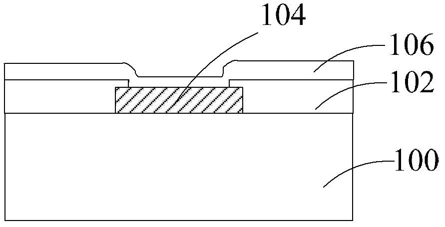
[0033] S101, forming an under bump metal layer on the pad and the passivation layer of the chip;

[0034] S102, forming a photoresist on the UBM layer, the photoresist having an opening to expose the UBM layer above the chip pad;

[0035] S103, forming a copper pillar on the UBM layer in the opening;

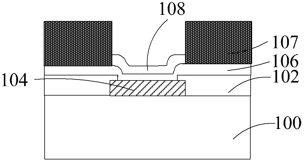
[0036] S104, forming solder bumps on the copper pillars;

[0037] S105, removing the photoresist;

[0038] S106, etching the UBM layer on the passivation layer until the passivation layer is exposed;

[0039] S107, forming an oxide layer on the surface of the exposed copper pillar;

[0040] S108 , removing oxides on the surface of the solder bumps, and reflowing the solder bumps.

[0041] First, step S101 is p...


PUM

PropertyMeasurementUnit
Thicknessaaaaaaaaaa
Thicknessaaaaaaaaaa
Thicknessaaaaaaaaaa

Abstract

A columnar bump packaging process comprises the following steps: forming lower metal bump layers on a welding pad and a passivation layer of a chip; forming photoresist on the lower metal bump layers, wherein the photoresist is provided with an opening so as to expose the lower metal bump layer above the welding pad of the chip; forming a copper column on the lower metal bump layer in the opening; forming a welding bump on the copper column; removing the photoresist; etching the lower metal bump layer on the passivation layer till the passivation layer is exposed; forming an oxide layer on the surface of the exposed copper column; and removing oxide on the surface of the welding bump, and refluxing the welding bump. The columnar bump packaging process of the invention improves the electrical performance and the reliability of the welding bump and is applicable to chip-level packaging of the welding pad with a dense spacing and multiple output functions.

Description

technical field [0001] The invention relates to the field of semiconductor device packaging, in particular to methods for forming flip-chip welding, solder bumps, and wafer-level chip scale packages (Wafer Level chip Scale Package, WLCSP). Background technique [0002] In recent years, since the microcircuit manufacturing of chips is developing toward high integration, the chip packaging also needs to develop in the direction of high power, high density, thinness and miniaturization. Chip packaging means that after the chip is manufactured, the chip is wrapped in plastic or ceramic materials to protect the chip from external moisture and mechanical damage. The main functions of the chip package are power distribution, signal distribution, heat dissipation and protection support. [0003] Since today's electronic products are required to be light, thin, small and highly integrated, the fabrication of integrated circuits will be miniaturized, resulting in an increase in the n...

Claims


Application Information

Patent Timeline
IPC IPC(8): H01L21/48
CPCH01L2224/11
Inventor 丁万春
Owner NANTONG FUJITSU MICROELECTRONICS
Why Eureka
Try Eureka