Gunn diode and manufacture method thereof
A Gunn diode and electrode technology, which is applied in the field of Gunn diode and its preparation, can solve the problems of unfavorable monolithic integration, failure to output oscillation frequency tuning, etc., and achieve easy monolithic integration, reduced dead zone, and simple preparation method Effect
- Summary
- Abstract
- Description
- Claims
- Application Information
AI Technical Summary
Problems solved by technology
Method used
Image
Examples
Embodiment Construction
[0038] The technical solution of the present invention will be described in detail below in conjunction with the accompanying drawings and embodiments.
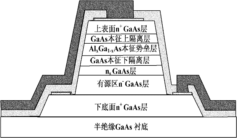
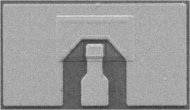
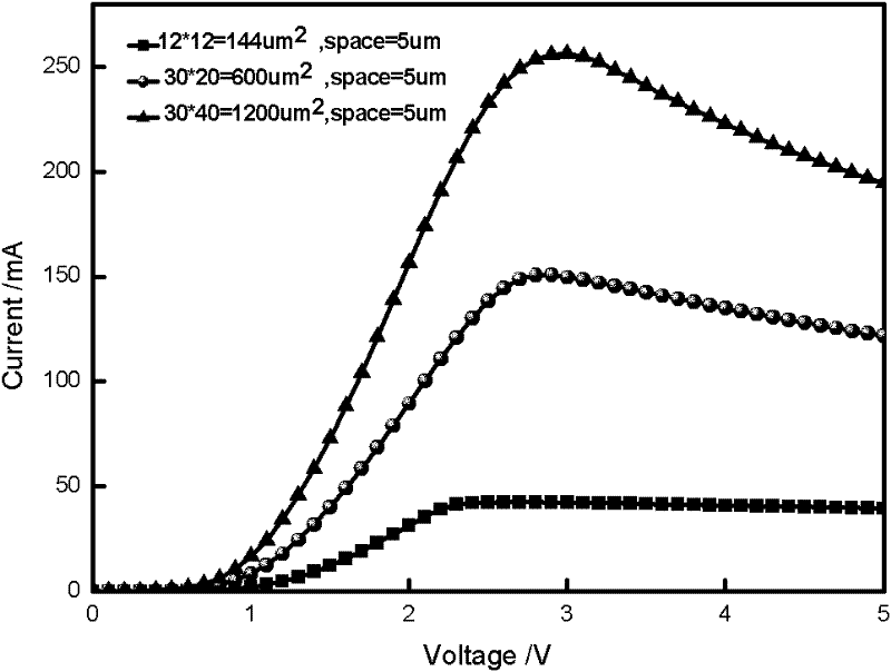
[0039] Such as figure 1 As shown, the embodiment of the present invention provides a Gunn diode, comprising: a semiconductor insulating GaAs substrate 1, a highly doped lower bottom surface n epitaxially grown on the semiconductor insulating GaAs substrate 1 + GaAs layer 2, located on the bottom surface under high doping n +Active region n epitaxially grown on GaAs layer 2 - GaAs layer 3, located in the active area n - Epitaxially grown n on the GaAs layer 3 s GaAs layer 4, located at n s GaAs intrinsic lower isolation layer 5 epitaxially grown on the GaAs layer 4, Al on the GaAs intrinsic lower isolation layer 5 epitaxially grown with a linear gradient of Al molar content x Ga 1-x As intrinsic barrier layer 6, located in Al x Ga 1-x The epitaxially grown GaAs intrinsic upper isolation layer 7 on the As intrinsic barr...
PUM
 Abstract
Description
Claims
Application Information


