MEMS (Micro Electro Mechanical System) capacitor based on three-dimensional silicon micro structure and manufacturing method thereof

A manufacturing method and capacitor technology, applied in capacitors, microstructure technology, fixed capacitors, etc., can solve the problems of low overload resistance, small capacity-to-volume ratio, poor environmental adaptability, etc., and achieve high safety, high energy storage density, low cost effect

Inactive Publication Date: 2012-07-11
ZHONGBEI UNIV
View PDF4 Cites 19 Cited by
  • Summary
  • Abstract
  • Description
  • Claims
  • Application Information

AI Technical Summary

Problems solved by technology

[0007] In order to solve the problems of low overload resistance, small capacity-to-volume ratio, poor environmental adaptability, and poor reliability of exist

Method used


Image

  • MEMS (Micro Electro Mechanical System) capacitor based on three-dimensional silicon micro structure and manufacturing method thereof
  • MEMS (Micro Electro Mechanical System) capacitor based on three-dimensional silicon micro structure and manufacturing method thereof
  • MEMS (Micro Electro Mechanical System) capacitor based on three-dimensional silicon micro structure and manufacturing method thereof

Examples


Embodiment Construction

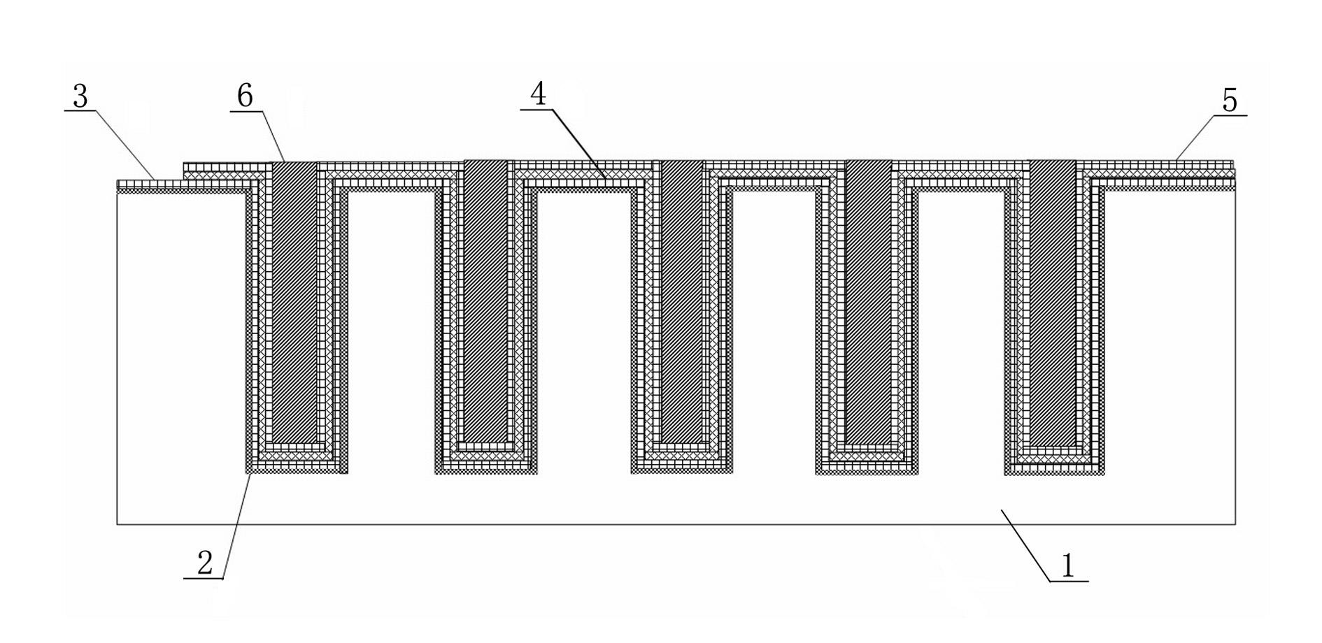
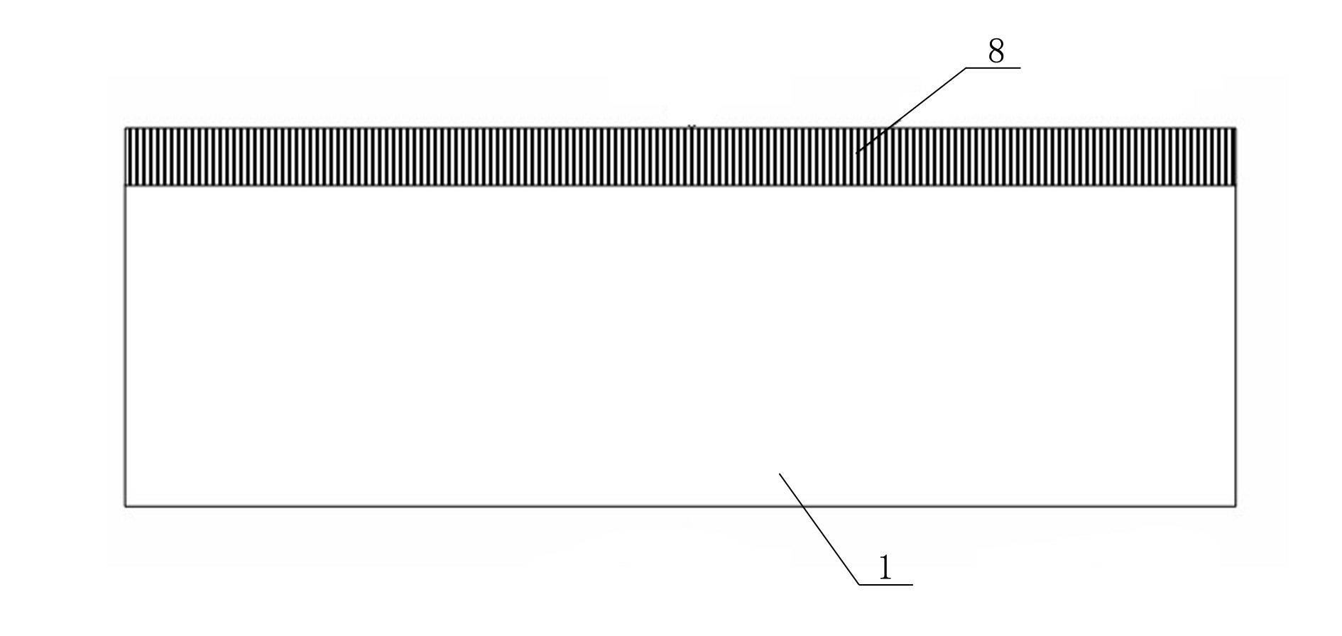
[0017] A MEMS capacitor based on a three-dimensional silicon microstructure, comprising a silicon substrate 1; the upper surface of the silicon substrate 1 is processed with a three-dimensional deep groove structure 7 with a large specific surface area; the upper surface of the silicon substrate 1 and the inner cavity surface of the three-dimensional deep groove structure 7 with a large specific surface area are formed There is an electrical insulating layer 2; a lower electrode layer 3 is formed on the upper surface of the electrical insulating layer 2; a dielectric layer 4 is formed on the upper surface of the lower electrode layer 3; an upper electrode layer 5 is formed on the upper surface of the dielectric layer 4; the lower electrode layer 3 is partially exposed to Outside the upper electrode layer 5; the micropores of the three-dimensional deep groove structure 7 with a large specific surface area are filled with a filling layer 6;

[0018] The material of the silicon su...


PUM


Abstract

The invention relates to a capacitor and a manufacturing technology thereof, in particular to an MEMS (Micro Electro Mechanical System) capacitor based on a three-dimensional silicon micro structure and a manufacturing method thereof, which solve the problems of low load resistance, small volume ratio, poor environmental suitability and poor reliability in the traditional MEMS micro capacitor. The MEMS capacitor based on the three-dimensional silicon micro structure comprises a silicon substrate, wherein a three-dimensional deep groove structure with big specific surface area is formed on the upper surface of the silicon substrate; electrical insulating layers are arranged on the upper surface of the silicon substrate and the cavity surface of the three-dimensional deep groove structure with big specific surface area; lower electrode layers are formed on the upper surfaces of the electric insulating layers; electric medium layers are formed on the upper surfaces of the lower electrode layers; upper electrode layers are formed on the upper surfaces of the electric medium layers; and the lower electrode layer parts are exposed out of the upper electrode layers. The MEMS capacitor based on the three-dimensional silicon micro structure is a full-solid electrostatic MEMS capacitor, which satisfies the development requirements of miniaturization, intellectualization and integration in the fields like fuse power supply, MEMS micro-energy, transportation and the like.

Description

technical field [0001] The invention relates to a capacitor and its manufacturing technology, in particular to a MEMS capacitor based on a three-dimensional silicon microstructure and its manufacturing method. Background technique [0002] Capacitors are the most basic and important electronic components in electronic equipment. They are widely used in key fields such as computers, communications, electric power, transportation, aviation, aerospace, and national defense. In the electronic equipment of ignition, timing, filtering, coupling, actuator power supply, uninterruptible power supply and other devices, capacitors play the role of storing and strengthening electric energy, and its stability and safety determine the reliable operation of the entire system. Therefore, capacitors, as reliable energy storage devices, have received increasing attention, especially microcapacitors are a hot research topic. Microcapacitors are new types of high-end power devices. Their devel...

Claims


Application Information

Patent Timeline
IPC IPC(8): H01G4/00H01G4/002H01G4/005H01G4/224B81C1/00
Inventor 丑修建熊继军陈旭远张文栋穆继亮郭茂香朱平
Owner ZHONGBEI UNIV
Why Eureka
Try Eureka