Laser diode assembly and semiconductor optical amplifier assembly
A technology of laser diodes and optical amplifiers, which is applied in the structure of semiconductor amplifiers, semiconductor lasers, and optical waveguide semiconductors, and can solve problems such as hindering the spread of laser technology and expensive solid-state laser light sources
Active Publication Date: 2012-07-11
SONY CORP +1
View PDF3 Cites 15 Cited by
- Summary
- Abstract
- Description
- Claims
- Application Information
AI Technical Summary
Problems solved by technology
However, titanium / sapphire lasers are expensive larger solid-state laser sources, which is the main factor hindering the spread of laser technology
Method used
View moreImage
Smart ImageViewing Examples

Examples
Embodiment 1
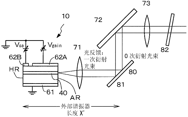
[0048] 2. Example 1 (laser diode assembly according to the embodiment of the present invention)
Embodiment 2
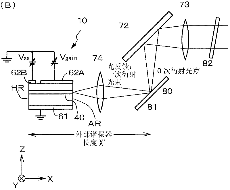
[0049] 3. Embodiment 2 (modified example of embodiment 1)
[0050] 4. Embodiment 3 (another modified example of Embodiment 1)
Embodiment 4
[0051] 5. Example 4 (semiconductor optical amplifier module according to the first embodiment of the present invention)
[0052] 6. Embodiment 5 (modified example of embodiment 4)
Login to View More PUM
| Property | Measurement | Unit |
|---|---|---|
| Thickness | aaaaa | aaaaa |
| Height | aaaaa | aaaaa |
| Width | aaaaa | aaaaa |
Abstract
The invention discloses a laser diode assembly and semiconductor optical amplifier assembly. The laser diode assembly includes a mode-locked laser diode device, where a light output spectrum shows long-wavelength shift by self-phase modulation, an external resonator, and a wavelength selective element (82,92,94-97). A long wavelength component of a pulsed laser beam emitted through the external resonator from the mode-locked laser diode device is extracted by the wavelength selective element, and output to the outside.
Description
technical field [0001] The present invention relates to laser diode assemblies and semiconductor optical amplifier assemblies. Background technique [0002] Today, ultrashort-pulse ultrahigh-power lasers are actively used for research in cutting-edge scientific fields using laser beams with pulse times of attoseconds or femtoseconds. Ultrashort-wave pulse lasers are actively studied from scientific interest in explaining ultrahigh-speed phenomena in picoseconds or femtoseconds, and further, practical applications of ultrashort-wave pulse lasers such as microfabrication or two-photon imaging using high peak power are actively studied. A high-power ultrashort-pulse laser diode device including a GaN-based compound semiconductor having an emission wavelength band of 405 nm is expected as a light source for a volumetric optical disk expected in a next-generation optical disk system after the Blu-ray optical disk system, in the medical field or in biological Light sources requir...
Claims
Login to View More Application Information
Patent Timeline
 IPC IPC(8): H01S5/065H01S5/14H01S5/068
CPCH01S5/0425H01S5/2009H01S5/101H01S5/06251H01S5/0657H01S5/16H01S5/0071H01S5/34333H01S5/22H01S5/50H01S5/028H01S5/3211H01S5/0064H01S5/309H01S5/0078H01S5/3216H01S5/141H01S5/1014H01S2301/176H01S5/3063H01S5/1085B82Y20/00H01S5/04252H01S5/04256
Inventor 横山弘之河野俊介仓本大
Owner SONY CORP