Nitride semiconductor laser

A technology of nitride semiconductors and lasers, which is applied in the direction of semiconductor lasers, lasers, laser components, etc., can solve problems that affect the work and life of lasers, uneven cavity surfaces of lasers, and enhanced cavity surface absorption, etc., to achieve simple structure and easy preparation, stress-reducing effect

Inactive Publication Date: 2012-07-11
苏州纳睿光电有限公司
View PDF6 Cites 26 Cited by
  • Summary
  • Abstract
  • Description
  • Claims
  • Application Information

AI Technical Summary

Problems solved by technology

[0004] In the nitride semiconductor laser with the above structure, there is a stress concentration area, that is, the interface between the upper InGaN waveguide and the p-AlGaN electron blocking layer, where the strain is relatively larg...

Method used


Image

  • Nitride semiconductor laser
  • Nitride semiconductor laser
  • Nitride semiconductor laser

Examples


Embodiment 1

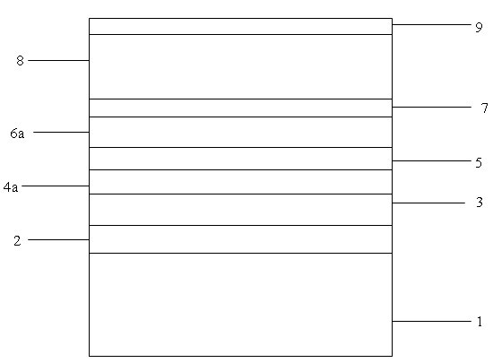
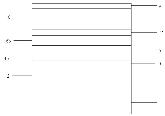
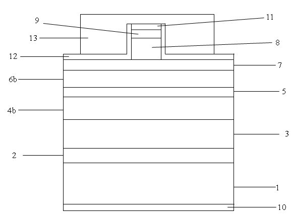
[0024] see Figure 2~4 As shown, a nitride semiconductor laser adopts a GaN-based blue laser, which is grown on a self-supporting GaN substrate 1 by MOCVD as figure 2 Structure shown, 2um thick n-GaN layer 2, 1um thick n-Al 0.16 Ga 0.84 N / GaN superlattice confinement layer 3, 140nm thick n-In x Ga 1-x N lower waveguide layer 4b, its In composition x linearly changes from 0 to 0.06, 5 cycles of In 0.17 Ga 0.83 N / n-GaN multi-quantum well active region 5, the well layer is not doped, the thickness is 2nm, the barrier layer is n-type doped, the thickness is 8nm, 100nm undoped gradient In y Ga 1-y N upper waveguide layer 6b, its In composition linearly changes from 0.06 to 0, 20nm thick p-Al 0.2 Ga 0.8 N electron blocking layer 7, 600nm thick p-Al 0.16 Ga 0.84 N / GaN optical confinement layer 8, p-GaN contact layer 9 with a thickness of 20nm.

[0025] After the epitaxial wafer is grown in MOCVD, rapid annealing is carried out in a nitrogen atmosphere of 800 °C for 20 min...


PUM


Abstract

The invention discloses a nitride semiconductor laser, which comprises sequentially a GaN substrate, a n-GaN layer, a n-AlGaN/GaN superlattice limiting layer, a lower InxGa1-xN gradual change waveguide layer, an InGaN/GaN multiple quantum well active area, an upper InyGa1-yN gradual change waveguide layer, a p-AlGaN electron barrier layer, a p-AlGaN/GaN superlattice limiting layer and a p-GaN contacting layer from bottom to top. In component content increases gradually from bottom to top in the lower InxGa1-xN gradual change waveguide layer and In component content decreases gradually from bottom to top in the upper InyGa1-yN gradual change waveguide layer. The nitride semiconductor laser can decrease the stress between an upper InGaN waveguide layer and the p-AlGaN electron barrier layer effectively, so that ragged steps can be avoided during cleavage. Simultaneously, the nitride semiconductor laser can strengthen optical limiting factors of the laser so as to improve performance of the laser effectively and acquire significant effect.

Description

technical field [0001] The invention relates to a nitride semiconductor laser, which belongs to the field of laser structure design in semiconductor technology. Background technique [0002] Nitride semiconductor lasers have the advantages of simple fabrication, small size, light weight, long life, and high efficiency, and are currently widely used in the fields of optical communication, optical pumping, optical storage, and laser display. [0003] At present, most nitride semiconductor lasers are F-P cavity semiconductor lasers, whose basic structure is GaN substrate, n-GaN layer, n-AlGaN / GaN superlattice confinement layer, lower InGaN waveguide layer, InGaN / GaN multiple quantum wells Active region, upper InGaN waveguide layer, p-AlGaN electron blocking layer, p-AlGaN / GaN superlattice confinement layer, p-GaN contact layer, such as figure 1 shown. In the manufacturing process of nitride semiconductor laser devices, it is necessary to cleavage the laser epitaxial wafer int...

Claims


Application Information

Patent Timeline
IPC IPC(8): H01S5/343H01S5/20
Inventor 冯美鑫张书明刘建平李增成杨辉
Owner 苏州纳睿光电有限公司
Why Eureka
Try Eureka