Nano imprinting device and method for imaging sapphire substrate

A sapphire substrate and nano-imprinting technology, which is applied to the exposure device of photoengraving process, photoengraving process of pattern surface, instruments, etc., can solve the problems of limited service life, high interfacial dislocation density, lattice mismatch, etc. , to achieve the effect of long service life, good light transmission performance and long service life of the mold

Active Publication Date: 2013-03-27
QINGDAO TECHNOLOGICAL UNIVERSITY
View PDF5 Cites 3 Cited by
  • Summary
  • Abstract
  • Description
  • Claims
  • Application Information

AI Technical Summary

Problems solved by technology

However, as the mainstream substrate in the LED industry, the sapphire substrate has a major defect: there is a large lattice mismatch and thermal stress mismatch with epitaxial materials such as GaN, which will cause a large number of defects in the epitaxial wafer (that is, due to crystal Lattice matching is low, resulting in high interfacial dislocation density)
[0007] Especially for the large-size whole wafer nanoimprinting process, good mold release ability determines the quality of the imprinted pattern and the service life of the mold. The existing hard molds used in nanoimprinting, such as silicon and quartz, must be surface-treated. Treatment, apply a layer of release agent, but the thinner release agent is easy to fall off during use, resulting in limited service life of the mold
Although soft molds, such as PDMS, have low surface energy and good mold release performance, they are prone to deformation during use and have a limited service life.
Frequent replacement is required, which affects production efficiency and is difficult to meet the production requirements of large-scale manufacturing in industrial applications

Method used


Image

  • Nano imprinting device and method for imaging sapphire substrate
  • Nano imprinting device and method for imaging sapphire substrate
  • Nano imprinting device and method for imaging sapphire substrate

Examples


Embodiment Construction

[0045] The present invention will be further described in detail below in conjunction with the accompanying drawings and the embodiments given by the inventor according to the technical solution of the present invention.

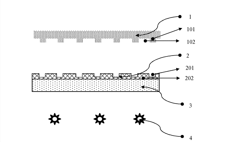
[0046] figure 1 , figure 2 , Figure 3A-Figure 3G with Figure 4A-Figure 4H , taking a 4-inch (about 100 mm) nano-patterned sapphire substrate 3 as an example, the implementation of wafer-level nano-patterning using the UV nanoimprint process based on a modified fluorocarbon resin-based hard polymer mold is described in detail. An imprinting device for a sapphire substrate and a manufacturing method thereof.

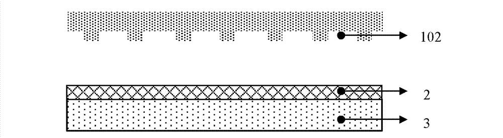
[0047] figure 1 Among them, a wafer-level nano-patterned sapphire substrate imprinting device, which includes: from top to bottom: a modified nano-imprint mold 1, a resist 2 for ultraviolet nano-imprinting, a sapphire substrate 3, UV light source 4 for exposure. Wherein, the resist 2 is coated on the sapphire substrate 3, the ultraviolet light s...


PUM

PropertyMeasurementUnit
diameteraaaaaaaaaa
depthaaaaaaaaaa
thicknessaaaaaaaaaa

Abstract

The invention discloses a nano imprinting device and method for imaging a sapphire substrate. The nano imprinting device comprises a nano imprinting mould, an ultraviolet nano imprinting resist, the sapphire substrate and an exposure ultraviolet light source, wherein the ultraviolet nano imprinting resist is spread on the sapphire substrate, the exposure ultraviolet light source is arranged below the sapphire substrate, and a characteristic cavity is arranged on the nano imprinting mould to form a characteristic image on the mould. By using a modified fluorocarbon resin-based hard polymer mould which has lowest surface energy and the advantages of a soft mould and a hard mould and better mechanical and physical performances and by combining the sapphire substrate which has better light transmission property relative to ultraviolet rays, the above-4 inch large-size wafer level nano imaged sapphire substrate is manufactured in a low-cost, high-productivity and large-scale manner. The invention can also be used for imaging other transparent substrates (such as a ZnO substrate).

Description

technical field [0001] The invention relates to a method for manufacturing a patterned sapphire substrate, in particular to a nano-imprinting device and method for patterning a sapphire substrate based on a modified fluorocarbon resin-based hard polymer mold, which realizes mass production of large-scale A wafer-level nano-patterned sapphire substrate belongs to the technical field of micro-nano manufacturing and optoelectronic device manufacturing. Background technique [0002] Sapphire substrate is currently the most important substrate for manufacturing GaN-based LEDs such as blue light, green light and white light. Compared with other substrates (such as silicon carbide, silicon, GaN, ZnO, etc.), it has mature manufacturing technology and low single-chip cost. , good chemical and temperature stability, good mechanical properties, no absorption of visible light and other advantages, it is currently the most widely used substrate in the LED industry. However, as the mains...

Claims


Application Information

Patent Timeline
Patent Type & Authority Patents(China)
IPC IPC(8): G03F7/00G03F7/20H01L33/00
Inventor 兰红波丁玉成
Owner QINGDAO TECHNOLOGICAL UNIVERSITY
Why Eureka
Try Eureka