Lamination differential photoelectric detector based on standard CMOS (complementary metal oxide semiconductor) process

A photodetector and process technology, applied in the field of photodetectors, can solve problems such as complex optical communication systems, input signal asymmetry, input load imbalance, etc., and achieve the effects of improving light injection efficiency, increasing working area, and simplifying structure

Inactive Publication Date: 2014-04-30
TIANJIN UNIV
View PDF4 Cites 0 Cited by
  • Summary
  • Abstract
  • Description
  • Claims
  • Application Information

AI Technical Summary

Problems solved by technology

In the current reports on differential structured optical receivers, or only one differential branch is connected to the photodetector, resulting in input signal asymmetry and input load imbalance; or two input optical signals are required, which makes the optical communication system complicated. At the same time, the cost is increased; or although one optical signal input is used, the two differential detectors each take half of the optical power, which reduces the utilization of the optical signal

Method used


Image

  • Lamination differential photoelectric detector based on standard CMOS (complementary metal oxide semiconductor) process
  • Lamination differential photoelectric detector based on standard CMOS (complementary metal oxide semiconductor) process

Examples


Embodiment Construction

[0015] In order to make the object, technical solution and advantages of the present invention clearer, the implementation manner of the present invention will be further described in detail below in conjunction with the accompanying drawings.

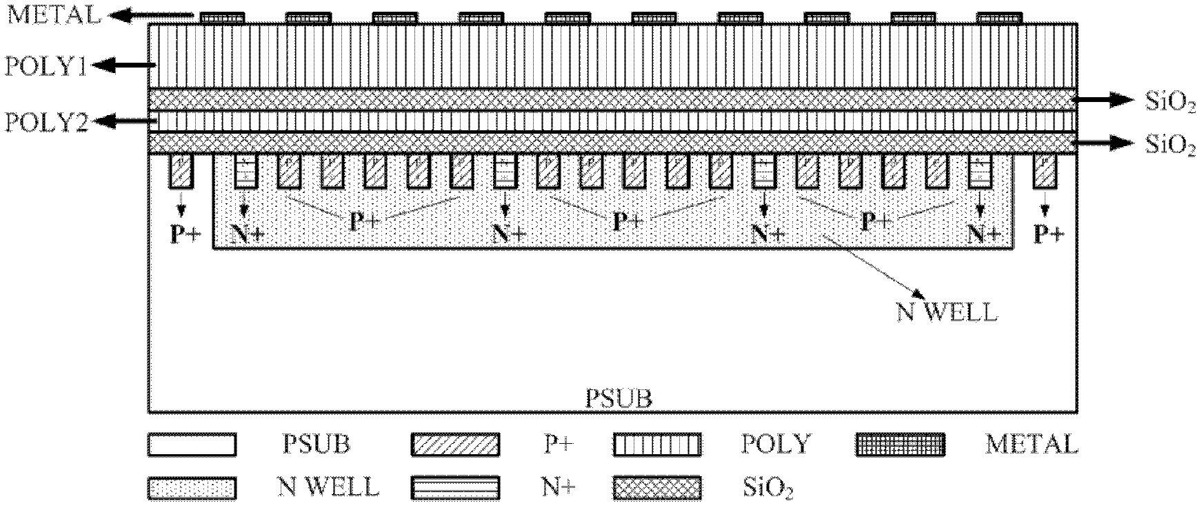
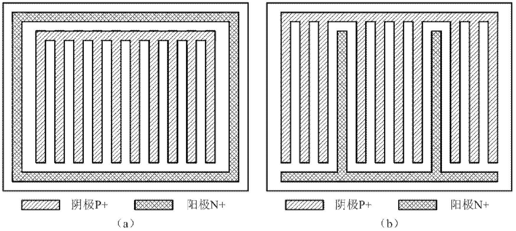
[0016] The laminated differential photodetector based on the standard CMOS process of the present invention comprises: an MSM type photodetector, a dual photodiode (DPD) type photodetector, and an isolation layer. The specific structure of the device is as figure 1 As shown, the MSM-PD is prepared on the polysilicon POLY1, and the double photodiode is prepared on the P-type substrate, and the two are separated by a layer of highly doped polysilicon (POLY2) sandwiched by two layers of SiO2. In the dual photodiode, the P+ / Nwell (N well) junction is used as the working diode, and the Nwell / Psub junction is used as the shielding diode to isolate the slow photogenerated carriers formed by the substrate. The SiO2 layer isolates the photo-ge...


PUM


Abstract

The invention relates to a lamination differential photoelectric detector based on a standard CMOS (complementary metal oxide semiconductor) process, belonging to the technical field of silicon-based optical receivers. The lamination differential photoelectric detector comprises an MSM type photoelectric detector, a dual-photodiode type photoelectric detector and an isolation layer arranged between the MSM type photoelectric detector and the dual-photodiode type photoelectric detector, wherein the MSM type photoelectric detector, the dual-photodiode type photoelectric detector and the isolation layer are arranged vertically, the dual-photodiode type photoelectric detector is manufactured on a silicon substrate PSUB, a P+ / N well junction is used as a working diode, an N well / Psub junction is used as a shielding diode, the dual-photodiode type photoelectric detector is positioned below the isolation layer, cathode P+ and anode N+ are alternatively arranged, the quantity of the cathodes P+ between every two adjacent anodes N+ is 3-4; and the MSM type photoelectric detector is positioned on a low-doped polycrystalline silicon layer POLY1 and positioned above the isolation layer. The lamination differential photoelectric detector provided by the invention can obtain two paths of mutually isolated photoelectric signals from one path of input optical signals; optical injection efficiency is increased; and enough responsiveness is obtained by an optical receiver based on the standard CMOS process under the condition of ensuring bandwidth and frequency characteristics.

Description

technical field [0001] The invention is applicable to the design of a silicon-based optical receiver, and relates to a photodetector based on a standard CMOS process. Background technique [0002] Photodetectors are the key components of optical receivers and are widely used in the field of optical communications. According to different working wavelengths, they are also widely used in special fields such as secure communications, environmental pollution monitoring, and non-invasive medical diagnosis. Different application environments have different requirements for photodetectors. For example, core communication networks and storage area networks require detectors to have very good frequency characteristics and performance, and are not sensitive to cost. In such applications, GaAs or InP-InGaAs-based photodetectors are generally used. Technology photodetector, this kind of detector performance is very good, but the cost is also very expensive. However, applications such a...

Claims


Application Information

Patent Timeline
Patent Type & Authority Patents(China)
IPC IPC(8): H01L27/144
Inventor 毛陆虹康玉琢肖新东张世林谢生
Owner TIANJIN UNIV
Why Eureka
Try Eureka