

Preparation method of silicon chip metallographic specimen
A technology of metallographic samples and silicon wafers, which is applied in the observation of microstructure, the preparation of metallographic samples of silicon wafers, and the preparation of metallographic samples of ultra-thin silicon wafers. Complete and unable to meet the problems of rapid sample preparation, to achieve the effect of improving stability and reliability and shortening sample preparation time
- Summary
- Abstract
- Description
- Claims
- Application Information
AI Technical Summary
Problems solved by technology
Method used
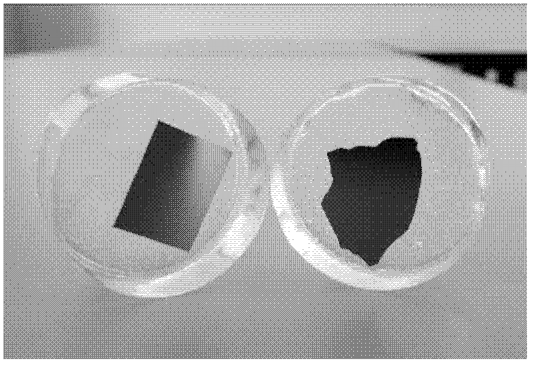
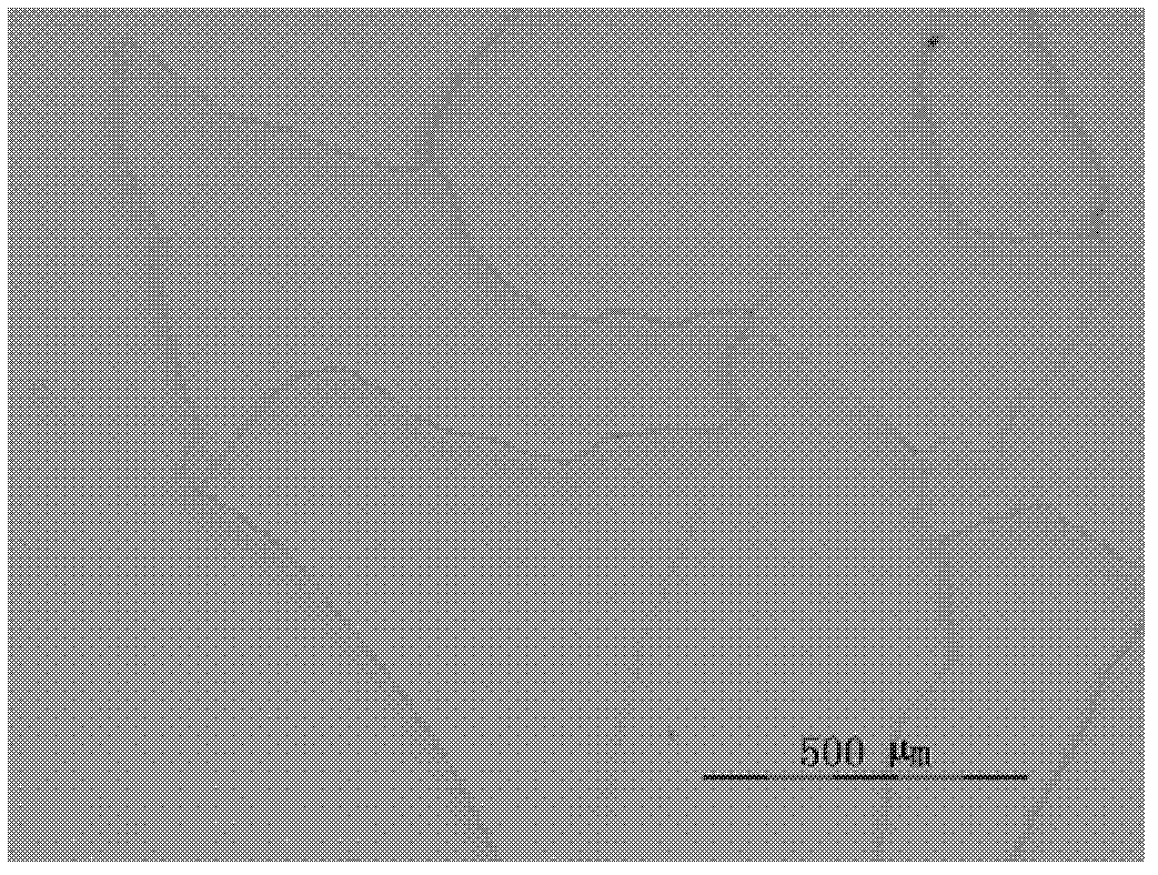
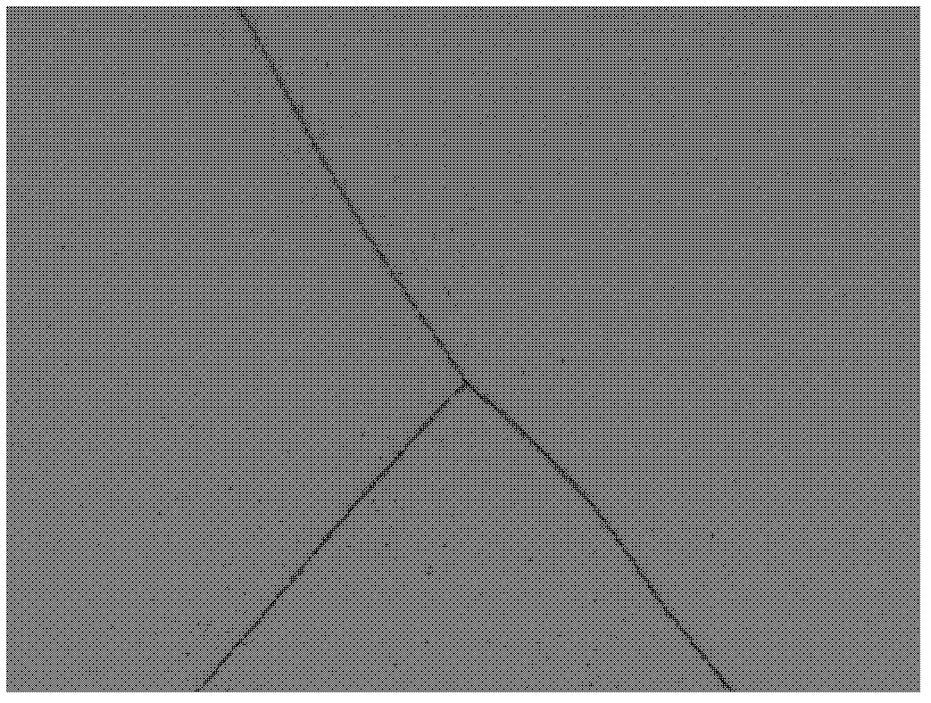
Image

Examples
Embodiment 1
[0033] The silicon wafer is an ultra-thin polycrystalline silicon wafer with a thickness of 180 μm. The preparation of the metallographic sample and the display steps of the microstructure are as follows:
[0034] 1) Mounting of samples: Mix acrylic resin powder and liquid curing agent according to the ratio (weight ratio 1:1) in the instructions for use, and stir slowly for about 1 min, add 10% (w / w) to the uniformly mixed solution ethanol and stir until uniform to make a cold mounting agent;
[0035] 2) Place a silicon wafer with a size of 15*20mm at the bottom of a silicone cold-mounting mold with an inner diameter of 40mm, and cast the cold-mounting agent of the above formula, and heat and cure at 25°C for 1 hour.
[0036] 3) Preliminarily polish the metallographic sample on a polishing machine. The polishing liquid is a diamond suspension with a particle size of 9 μm and 3 μm for 4 minutes respectively. The polishing process uses single-point loading with a pressure of 15...
Embodiment 2
[0045] The same as the preparation method in Example 1, the difference is that in step 1), 5% (w / w) ethanol is added to the homogeneously mixed solution and stirred until uniform to prepare a cold mounting agent.
Embodiment 3
[0047] The same as the preparation method of Example 1, the difference is that in step 1), 25% (w / w) ethanol is added to the homogeneously mixed solution and stirred until uniform to prepare a cold mounting agent.
PUM
| Property | Measurement | Unit |
|---|---|---|
| thickness | aaaaa | aaaaa |
| particle diameter | aaaaa | aaaaa |
| thickness | aaaaa | aaaaa |
Abstract
Description
Claims
Application Information