Surface enhanced Raman scattering (SERS) substrate and preparation method thereof
A surface-enhanced Raman and substrate technology, applied in Raman scattering, material excitation analysis, etc., can solve the problems of low concentration of the aqueous solution of the analyte, high technical difficulty, and unfavorable promotion.
- Summary
- Abstract
- Description
- Claims
- Application Information
AI Technical Summary
Problems solved by technology
Method used
Image
Examples
preparation example Construction
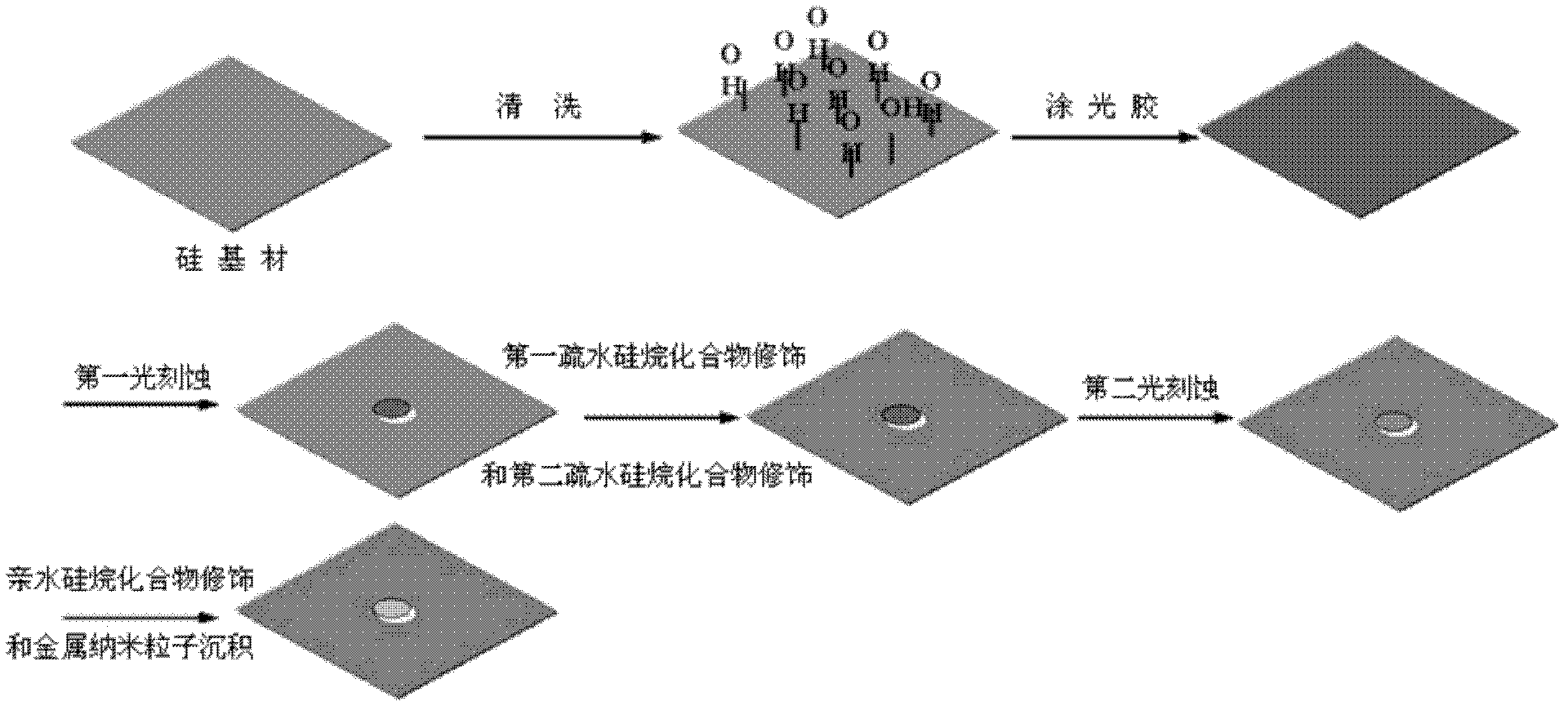
[0043] The present invention provides a method for preparing a surface-enhanced Raman substrate described in the above technical solution, comprising the following steps:
[0044] a) using the template as a mask layer to perform first photoetching on the silicon substrate and modifying it with a hydrophobic silane compound to obtain a silicon substrate comprising a hydrophobic silane compound layer;
[0045] b) The silicon substrate obtained in the step a) is subjected to the second photoetching exposure and then modified with a hydrophilic silane compound to obtain a silicon substrate comprising a hydrophilic silane compound layer and a hydrophobic silane compound layer, and the hydrophobic silane The compound layer surrounds the hydrophilic silane compound layer, and the area of the hydrophilic silane compound layer is less than 7.5mm 2 ;
[0046] c) depositing metal nanoparticles on the hydrophilic silane compound layer of the silicon substrate obtained in step b) to obt...
Embodiment 1
[0077] according to figure 1 In the process flow shown, a circle with a diameter of 2 mm is used as a template, octadecyl trichlorosilane is the first hydrophobic silane compound, n-propyl triethoxysilane is the second hydrophobic silane compound, aminopropyl triethoxy The base silane is a hydrophilic silane compound, and silver nanoparticles are selected as metal nanoparticles to obtain a surface-enhanced Raman scattering substrate.
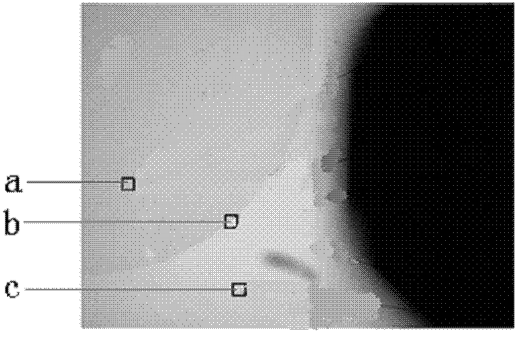
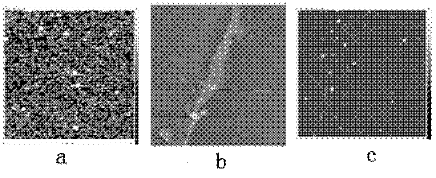
[0078] The present invention carries out optical test with the obtained surface-enhanced Raman scattering substrate, and the results are as follows: figure 2 and image 3 as shown, figure 2 The optical photo of the surface-enhanced Raman scattering substrate provided by Example 1 of the present invention, wherein a is the central region of the substrate, b is the junction of the central region and the surrounding region, and c is the surrounding region, by figure 2 It can be seen that the surface-enhanced Raman scattering substrate provide...
PUM
| Property | Measurement | Unit |
|---|---|---|
| Area | aaaaa | aaaaa |
| Diameter | aaaaa | aaaaa |
Abstract
Description
Claims
Application Information


