Method for detecting minority carrier lifetime of semiconductor nanowire

A technology of minority carrier and detection method, applied in the field of detection of low-dimensional structure semiconductor materials, can solve the problems of nanowire optoelectronic performance degradation, high process requirements and cost, and short diffusion length of hundreds to tens of nanometers.

Active Publication Date: 2015-01-07
SHANGHAI INST OF TECHNICAL PHYSICS - CHINESE ACAD OF SCI
View PDF5 Cites 0 Cited by
  • Summary
  • Abstract
  • Description
  • Claims
  • Application Information

AI Technical Summary

Problems solved by technology

The relative deficiencies and limitations of this type of method are: 1) It is necessary to prepare a single nanowire device, the process requirements and costs are high, and the process such as photolithography, corrosion, etc. will cause the decline of the photoelectric performance of the nanowire, resulting in the extraction of parameters possible departure from the original properties of the nanowire
3) The resolution of this method to measure the minority carrier diffusion length of nanowires depends on the spot diameter, and it is powerless when the minority carrier diffusion length to be measured is close to or even smaller than the excitation spot size (shorter minority carrier lifetime)
For direct bandgap semiconductor nanostructures, the minority carrier lifetime is often at the level of nanoseconds or even picoseconds, and the diffusion length is as short as hundreds to tens of nanometers.

Method used


Image

  • Method for detecting minority carrier lifetime of semiconductor nanowire
  • Method for detecting minority carrier lifetime of semiconductor nanowire
  • Method for detecting minority carrier lifetime of semiconductor nanowire

Examples


Embodiment Construction

[0014] Taking GaAs nanowires as an example below, the specific implementation manner of the present invention will be described in detail in conjunction with the accompanying drawings.

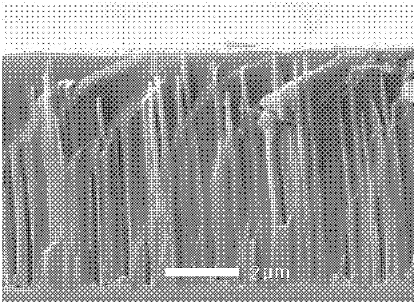
[0015] The preparation of nanowire samples includes spin-coating, baking, polishing and other steps. Firstly, a uniform layer of polymer (refractive index lower than the nanowire material, thickness slightly higher than the height of the nanowire) is spin-coated on the upper surface of the sample by mechanical spin coating; then the wrapped sample is baked to make it completely Curing; Finally, the wrapping at the top is removed by polishing and thinning, so that the top of the nanowire is exposed to meet the measurement requirements. The SEM picture of the sample section prepared in this embodiment is as follows: figure 1 shown.

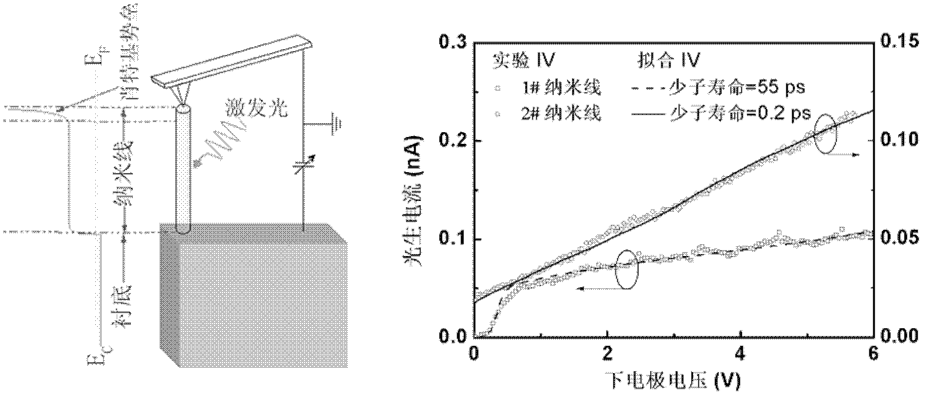
[0016] figure 2 It is a schematic diagram of the present invention for measuring the photocurrent of a single nanowire. If the substrate or buffer layer of the...


PUM


Abstract

The invention discloses a method for detecting the minority carrier lifetime of a semiconductor nanowire. The method comprises the following steps of: measuring the light excitation current response of a single nanowire under Schottky reverse bias by using a conductive scanning probe, performing quantitative fitting on a light current-bias curve by using a numerical model, and determining the minority carrier lifetime of the semiconductor nanowire. The method is suitable for measuring the carrier dynamic characteristic of the single nanowire in a nanowire sample prepared by an epitaxial method, an etching method and the like; and light excitation intensity is low, and the working state of the nanowire in a photoelectric device is approached, so the method has great significance for analyzing and evaluating the core performance of the nanowire and the photoelectric device.

Description

technical field [0001] The invention relates to the detection of low-dimensional structure semiconductor materials, in particular to a novel measurement method for the lifetime of minority carriers of semiconductor nanowires. Background technique [0002] Semiconductor nanowires have gained considerable attention in the fields of photodetection and solar energy harvesting due to their unique structures and optoelectronic properties. The minority carrier lifetime (hereinafter referred to as the minority carrier lifetime) is the main factor determining the photoelectric performance of the device. Due to the high surface-to-volume ratio of nanowires, surface scattering has a significant impact on their minority carrier lifetimes, which is very different from bulk materials. Therefore, the extraction of the lifetime of a single nanowire has very positive significance for the optimization of its material properties and the performance improvement and application of devices. [...

Claims


Application Information

Patent Timeline
Patent Type & Authority Patents(China)
IPC IPC(8): G01R31/26
Inventor 李天信夏辉陆卫胡伟达姚碧霂黄文超
Owner SHANGHAI INST OF TECHNICAL PHYSICS - CHINESE ACAD OF SCI
Why Eureka
Try Eureka