High reliability soi LDMOS power device

A power device, a reliable technology, applied in the field of highly reliable SOILDMOS power devices, can solve problems such as poor reliability, achieve the effect of raising the maintenance voltage, avoiding damage or burning of LDMOS devices, and expanding the electrical safe working area

Active Publication Date: 2016-05-04
BEIJING YANDONG MICROELECTRONICS
View PDF5 Cites 0 Cited by
  • Summary
  • Abstract
  • Description
  • Claims
  • Application Information

AI Technical Summary

Problems solved by technology

[0004] The purpose of the present invention is to solve the problem of poor reliability of SOILDMOS power devices in the prior art and provide a highly reliable SOILDMOS power device

Method used


Image

  • High reliability soi LDMOS power device
  • High reliability soi LDMOS power device
  • High reliability soi LDMOS power device

Examples


Embodiment 1

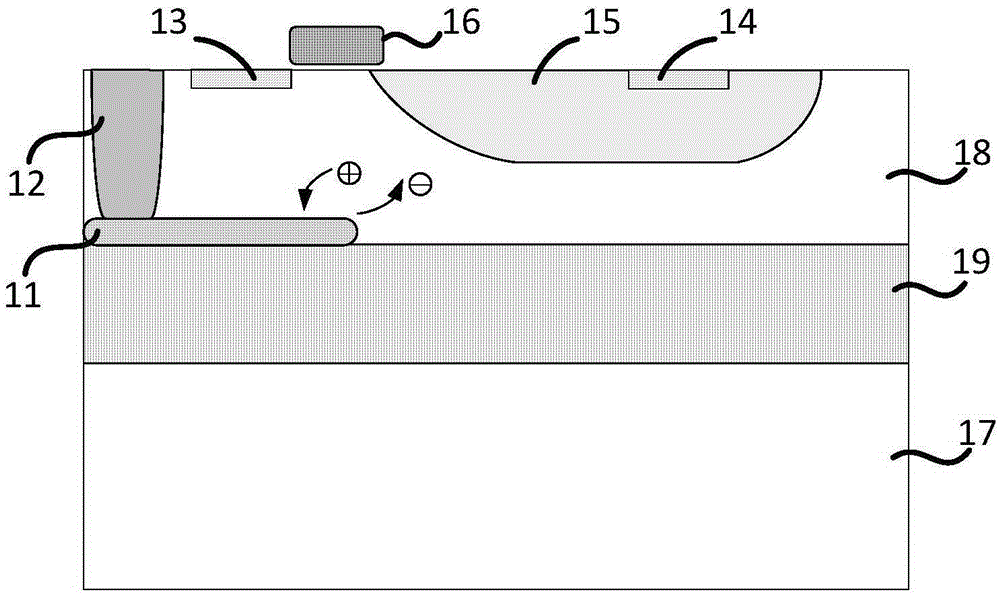
[0028] The highly reliable SOILDMOS power device provided by the present invention, such as figure 1 As shown, in the figure, 19 is a buried oxide layer, and the material is silicon dioxide; 18 is a top silicon layer, in which an SOI device is fabricated; 17 is a bottom silicon layer, which is completely isolated from the top silicon layer 18 by the buried oxide layer 19 16 is the SOILDMOS gate, the material is polysilicon implanted with high concentration; 15 is the drift region; 13 is the source implantation region to form the device source, 14 is the drain implantation region to form the device drain; 11 is the buried layer, in this embodiment Its range is a part of the working area of ​​the device, and the depth is close to the buried oxide layer 19 above the buried oxide layer 19; 12 is a high-concentration contact injection region, and its function is to connect the surface of the buried layer 11 and the top silicon layer 18, so that the buried layer 11 The potential of ...

Embodiment 2

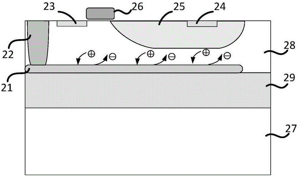
[0030] Such as figure 2 As shown, it is a schematic cross-sectional view of a SOILDMOS power device structure in which the buried oxide layer is next to the buried oxide layer and the entire working area is buried in the embodiment of the present invention. In the figure, 29 is a buried oxide layer, and the material is silicon dioxide; 28 is a top silicon layer, in which an SOI device is fabricated; 27 is a bottom silicon layer, which is completely isolated from the top silicon layer 28 by a buried oxide layer 29; 26 is SOILDMOS gate, the material is the polysilicon of high-concentration implantation; 25 is the drift region; 23 is the device source end that the source end implantation region forms, and 24 is the drain end implantation region and forms the device drain end; 21 is the buried layer, and its scope is in this embodiment The entire working area of ​​the device has a depth that is close to the buried oxide layer 29 above the buried oxide layer 29; 22 is a high-conce...

Embodiment 3

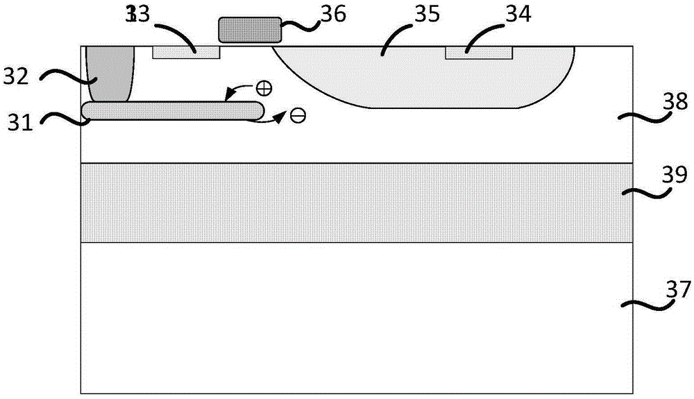
[0032] Such as image 3 As shown, it is a schematic cross-sectional view of a SOILDMOS power device structure in which the buried oxide layer and the device surface are partially buried in the working region according to an embodiment of the present invention. 39 is a buried oxide layer, the material is silicon dioxide; 38 is a top silicon layer, in which an SOI device is made; 37 is a bottom silicon layer, which is completely isolated from the top silicon layer 38 by a buried oxide layer 39; 36 is a SOILDMOS gate, The material is high-concentration implanted polysilicon; 35 is the drift region; 33 is the source implantation region to form the device source, 34 is the drain implantation region to form the device drain; 31 is the buried layer, and its scope is the device working area in this embodiment 32 is a high-concentration contact injection region, and its function is to connect the surface of the buried layer 31 and the top silicon layer 38, so that the potential of the ...


PUM


Abstract

Disclosed is a high-reliability silicon-on-insulator (SOI) laterally diffused metal oxide semiconductor (LDMOS) power element, which comprises a buried layer with high concentration and a contact injection region, wherein the buried layer with high concentration and the contact injection region are injected in top layer silicon of the SOI LDMOS power element, and the buried layer is connected with the contact injection region; current carriers which are located near a SOI LDMOS gate in the SOI LDMOS power element can be extracted through the buried layer and educed through the contact injection region, and electric potentials which are near the SOI LDMOS gate can be controlled. According to the high-reliability SOI LDMOS power element, in the top layer silicon of the SOI LDMOS, the buried layer with high concentration is produced and educed through the contact injection region, the current carriers which are located near the SOI LDMOS gate in the SOI LDMOS power element can be extracted through the buried layer, the electric potentials which are near the gate can be controlled, so that damages or burning of LDMOS elements caused by the fact that parasitic transistors open due to noise current or colliding current, maintaining voltage of the LDMOS elements under static shock is raised simultaneously, electrical safety working areas of the LDMOS power elements are expanded, and reliability of the elements is strengthened.

Description

technical field [0001] The invention relates to the field of semiconductor manufacturing, in particular to a highly reliable SOILDMOS power device. Background technique [0002] LDMOS (LateralDoubleDiffusedMetalOxideSemiconductorFieldEffectTransistor, lateral double-diffused metal oxide field effect transistor) has high gain, wide linear range, and low intermodulation distortion, and is widely used in various fields such as wireless communication and medical electronics. The longitudinal electric field of the SOI device structure is small, the inversion layer is thicker, the surface scattering effect is reduced, the mobility of the device is high, and the transconductance is large. In addition, the parasitic capacitance mainly comes from the capacitance of the buried silicon dioxide layer, which is much smaller than that in the bulk silicon MOSFET. Capacitance does not change with the scaling down of the device, and the junction capacitance and connection capacitance of SOI ...

Claims


Application Information

Patent Timeline
Patent Type & Authority Patents(China)
IPC IPC(8): H01L29/78H01L29/06
Inventor 姜一波杜寰
Owner BEIJING YANDONG MICROELECTRONICS
Why Eureka
Try Eureka