Use of photochromic cadmium sulfide comb-shaped semiconductor micro-nano material
A technology of micro-nano materials and photochromism, which is applied in the direction of color-changing fluorescent materials, fiber raw material processing, chemical instruments and methods, etc., to achieve the effects of rich color changing range, simple production, and wide source of raw materials
- Summary
- Abstract
- Description
- Claims
- Application Information
AI Technical Summary
Problems solved by technology
Method used
Image

Examples
Embodiment 1
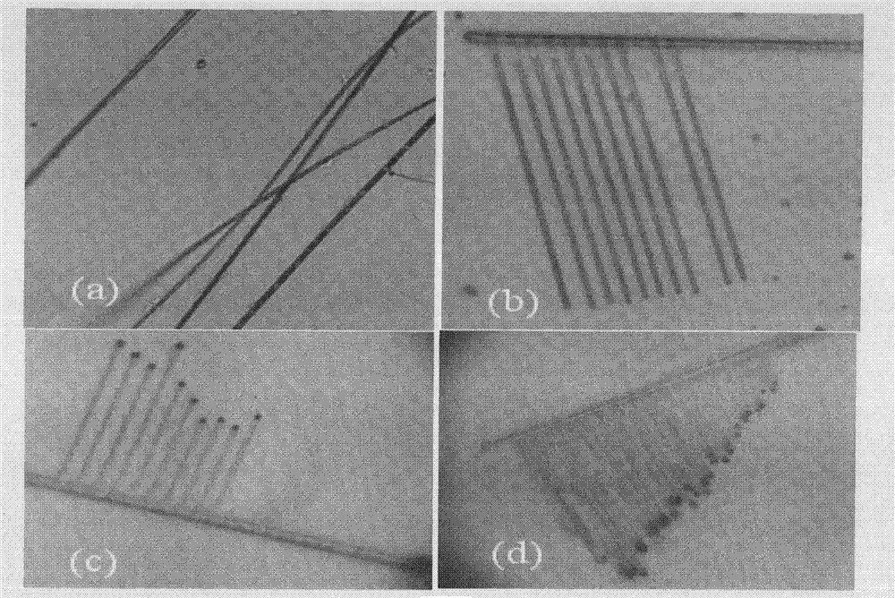
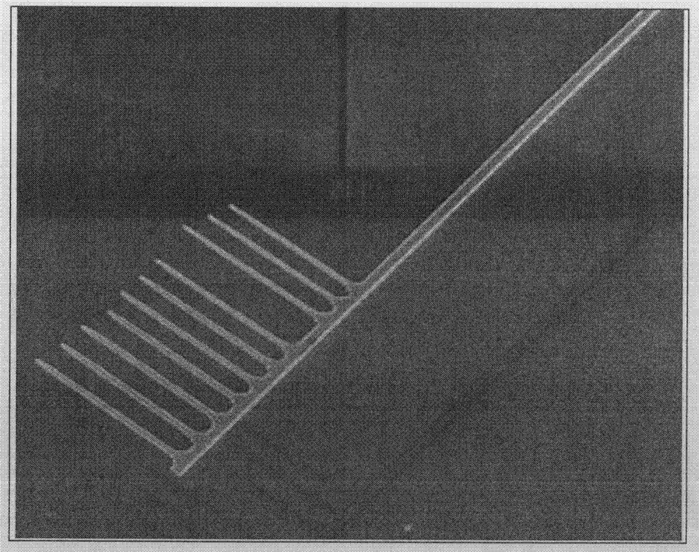
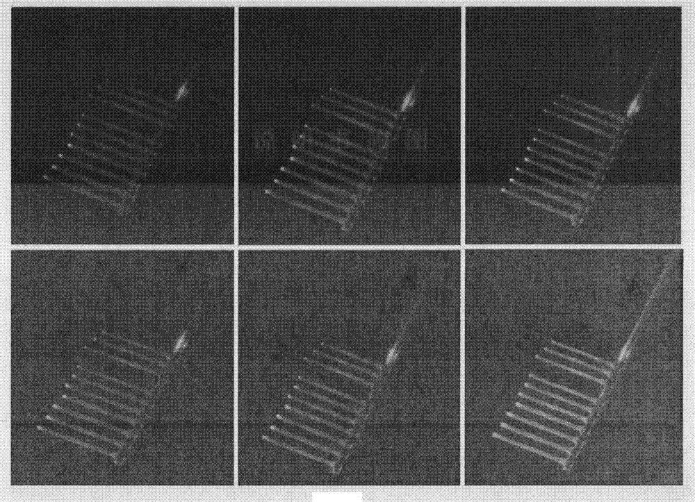
[0027] A kind of cadmium sulfide comb semiconductor micro-nano material, this material is cadmium sulfide (CdS) doped with tin (Sn), calculated with the amount of the total substance of this material, with transmission electron microscope (TEM) or scanning electron microscope (SEM) The equipped energy spectrometer can characterize the molar content of tin within 1%.
[0028] A preparation method of cadmium sulfide comb semiconductor micro-nano material, the steps are: uniformly stirring cadmium sulfide and tin dioxide in a mortar for 10 minutes according to the molar ratio of 100:8; Clean it in the oven for 10 minutes, and after drying, use an ion sputtering device to plate gold for 60 seconds, and clean the porcelain boat and quartz tube for later use. Then put CdS and SnO 2Put the mixture into a porcelain boat, and place the porcelain boat in the center of the quartz tube. A gold-plated silicon wafer was placed in another porcelain boat, placed upstream of the gas flow of ...
Embodiment 2
[0030] A preparation method of cadmium sulfide comb semiconductor micro-nano material, the steps are: uniformly stirring cadmium sulfide and tin dioxide in a mortar for 10 minutes according to the molar ratio of 100:10; Clean it in the oven for 10 minutes, and after drying, use an ion sputtering device to plate gold for 60 seconds, and clean the porcelain boat and quartz tube for later use. Then put CdS and SnO 2 Put the mixture into a porcelain boat, and place the porcelain boat in the center of the quartz tube. A gold-plated silicon wafer was placed in another porcelain boat, placed upstream of the gas flow of the quartz tube, 11 cm from the center of the quartz tube. Put the quartz tube into the tube furnace. The upstream of the quartz tube is first connected to the flow meter, then connected to the exhaust system, and the downstream is connected to the exhaust gas treatment system, and then the mixed gas of argon and hydrogen is introduced. After exhausting for one hour, ...
Embodiment 3
[0036] A preparation method of cadmium sulfide comb semiconductor micro-nano material, the steps are: uniformly stirring cadmium sulfide and tin dioxide in a mortar for 10 minutes according to the molar ratio of 100:12; Clean it in the oven for 10 minutes, and after drying, use an ion sputtering device to plate gold for 60 seconds, and clean the porcelain boat and quartz tube for later use. Then put CdS and SnO 2 Put the mixture into a porcelain boat, and place the porcelain boat in the center of the quartz tube. A gold-plated silicon wafer was placed in another porcelain boat, placed upstream of the gas flow of the quartz tube, 11 cm from the center of the quartz tube. Put the quartz tube into the tube furnace. The upstream of the quartz tube is first connected to the flow meter, then connected to the exhaust system, and the downstream is connected to the exhaust gas treatment system, and then the mixed gas of argon and hydrogen is introduced. After exhausting for one hour, ...
PUM
| Property | Measurement | Unit |
|---|---|---|
| diameter | aaaaa | aaaaa |
Abstract
Description
Claims
Application Information
 - R&D
- Intellectual Property
- Life Sciences
- Materials
- Tech Scout
- Unparalleled Data Quality
- Higher Quality Content
- 60% Fewer Hallucinations
Browse by: Latest US Patents, China's latest patents, Technical Efficacy Thesaurus, Application Domain, Technology Topic, Popular Technical Reports.
© 2025 PatSnap. All rights reserved.Legal|Privacy policy|Modern Slavery Act Transparency Statement|Sitemap|About US| Contact US: help@patsnap.com