Preparation method of resistance random access memory and resistance random access memory

A technology of resistive memory and resistive layer, applied in semiconductor devices, electric solid devices, electrical components, etc., can solve the problems of limiting the application range of resistive memory, high cost, increasing manufacturing cost, etc., to achieve good characteristics and reliability. , The effect of simple equipment and cost reduction

Active Publication Date: 2012-09-05
PEKING UNIV
View PDF3 Cites 5 Cited by
  • Summary
  • Abstract
  • Description
  • Claims
  • Application Information

AI Technical Summary

Problems solved by technology

[0003] Resistive variable memory is a two-terminal device structure, so it is easy to manufacture a cross-array structure to achieve high-density memory, but because the traditional semiconductor process uses silicon wafers as substrates, sputtering, photolithography and etching processes are required, and the cost is very high , limiting the scope of application of resistive memory
Especially when using cross-array resistive memory to realize a three-dimensional memory, multiple photolithography will be used to greatly increase the manufacturing cost

Method used


Image

  • Preparation method of resistance random access memory and resistance random access memory
  • Preparation method of resistance random access memory and resistance random access memory
  • Preparation method of resistance random access memory and resistance random access memory

Examples


Embodiment Construction

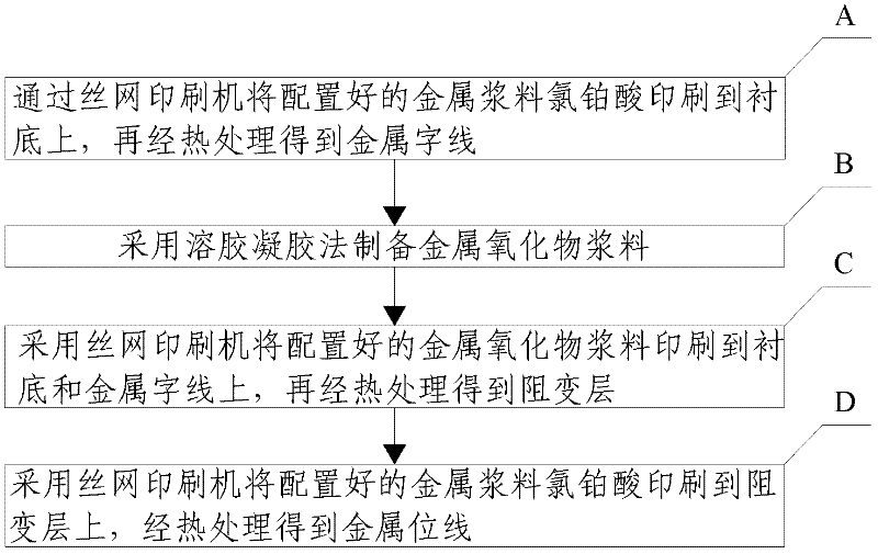
[0031] The specific implementation manners of the present invention will be further described in detail below in conjunction with the accompanying drawings and embodiments. The following examples are used to illustrate the present invention, but are not intended to limit the scope of the present invention.

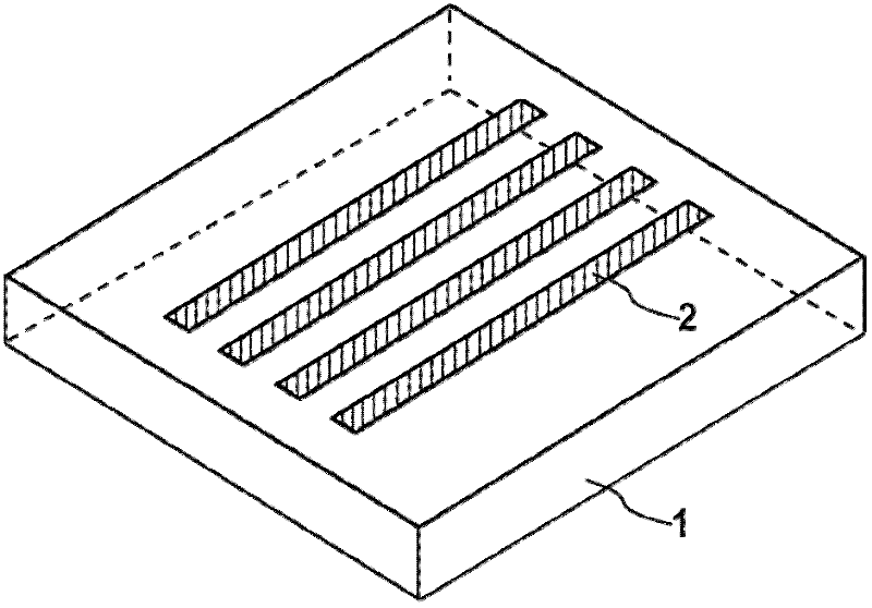
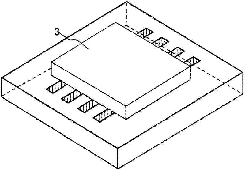
[0032] The cross-array structure of RRAM has been extensively studied, but the method of fabricating 3D structured RRAM using screen printing combined with sol-gel method has not been proposed yet.

[0033] Among them, the basic principle of screen printing is: use the basic principle that the screen graphics part of the mesh is transparent to the slurry, and the non-graphic part of the mesh is impermeable to the slurry for printing. When printing, pour the slurry at one end of the screen, apply a certain pressure on the slurry part of the screen with a scraper, and move towards the other end of the screen at the same time. The slurry is squeezed from the mesh of the grap...


PUM


Abstract

The invention discloses a preparation method of a resistance random access memory and the resistance random access memory. The preparation method comprises the following steps of: (A) printing prepared metal slurry chloroplatinic acid on a substrate by a silk-screen printing machine, and carrying out heat treatment to obtain metal word line; (B) preparing metal oxide slurry by adopting a sol-gel method; (C) printing the prepared metal oxide slurry on the substrate and the metal word lines by adopting the silk-screen printing machine, and carrying out heat treatment to obtain a resistance layer; and (D) printing the prepared metal slurry chloroplatinic acid on the resistance layer by adopting the silk-screen printing machine and carrying out heat treatment to obtain a metal position line. The preparation method has the advantages that the resistance random access memory array is manufactured by adopting a method for combination of the sol-gel method and the silk-screen printing, and the traditional semiconductor manufacturing process is not used, so that the cost is reduced, the requirement for the process conditions is low, the equipment is simple, the process flow adopts low temperature and can be compatible to various substrate materials and processes, and the resistance random access memory prepared by the method is better in characteristic and reliability.

Description

technical field [0001] The invention relates to the technical field of semiconductor integrated circuits and their manufacture, in particular to a preparation method of a resistive variable memory and the resistive variable memory. Background technique [0002] At present, a new type of non-volatile memory based on the principle of resistance change storage has become the next-generation semiconductor memory because of its advantages of high speed (<5ns), low operating voltage (<1V), high storage density, and easy integration. strong competitor. This kind of device called "resistive variable memory (RRAM)" generally has a metal-insulator-metal structure, that is, a layer of dielectric film material with resistive properties is added between two layers of metal electrodes. These resistive materials generally It is a metal oxide, the common ones are NiO, TiO 2 , HfO 2 , ZrO 2 、WO 3 and Ta 2 o 5 etc. The working mode of resistive variable memory includes unipolar ...

Claims


Application Information

Patent Timeline
IPC IPC(8): H01L45/00H01L27/24
Inventor 刘力锋于迪陈冰王琰傅亦晗韩德栋王漪刘晓彦康晋锋张兴
Owner PEKING UNIV
Why Eureka
Try Eureka