High-temperature annealing method for manufacturing silicon carbide device

A high-temperature annealing, silicon carbide technology, applied in semiconductor/solid-state device manufacturing, electrical components, circuits, etc., to achieve the effects of low production cost, shortened process time, and reduced annealing time

Active Publication Date: 2012-09-12
NO 55 INST CHINA ELECTRONIC SCI & TECHNOLOGYGROUP CO LTD
View PDF2 Cites 11 Cited by
  • Summary
  • Abstract
  • Description
  • Claims
  • Application Information

AI Technical Summary

Problems solved by technology

The currently commonly used SiC high-temperature annealing method still has many defects, and the preparation of the protective layer and the annealing conditions still need to be improved.

Method used


Image

  • High-temperature annealing method for manufacturing silicon carbide device
  • High-temperature annealing method for manufacturing silicon carbide device

Examples


Embodiment 1

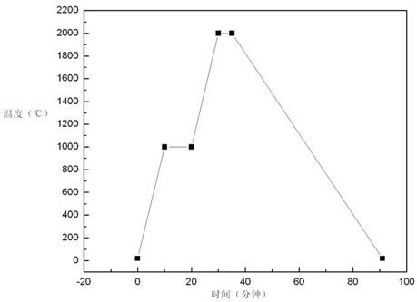
[0020] With reference to the accompanying drawings,

[0021] 1) Use a mixed solution of hydrochloric acid and nitric acid (the weight ratio is 1:1) to clean the ion-implanted SiC wafer, type 4H-SiC;

[0022] 2) Coating a layer of ArF photoresist on the SiC wafer as a protective layer;

[0023] 3) Put the SiC wafer into a high-temperature annealing furnace, and fill it with argon as a protective gas;

[0024] 4) Set the pressure of the high-temperature annealing furnace to 10Pa, heat the SiC wafer to 1000°C for the first time, and heat up at a rate of 100°C / min, keep the temperature for 10 minutes, and carbonize the protective layer;

[0025] 5) Set the pressure of the high-temperature annealing furnace to 1000Pa, heat the SiC wafer for the second time, from 1000°C to 2000°C, with a heating rate of 100°C / min, keep the temperature for 1 minute, and perform high-temperature annealing;

[0026] 6) Set the pressure of the high-temperature annealing furnace to 2000Pa, and cool dow...

Embodiment 2

[0028] Referring to the accompanying drawings,

[0029] 1) Clean the ion-implanted SiC wafer with sulfuric acid, then clean the ion-implanted SiC wafer with hydrochloric acid, type 6H-SiC;

[0030] 2) Coating a layer of electron beam photoresist on the SiC wafer as a protective layer;

[0031] 3) Put the SiC wafer into a high-temperature annealing furnace, and fill it with argon as a protective gas;

[0032] 4) Set the pressure of the high-temperature annealing furnace to 0.0001Pa, heat the SiC wafer for the first time to 850°C, the heating rate is 80°C / min, and keep the temperature for 30 minutes to carbonize the protective layer;

[0033] 5) Set the pressure of the high-temperature annealing furnace to 500Pa, heat the SiC wafer for the second time, from 850°C to 1850°C, with a heating rate of 200°C / min, keep the temperature for 5 minutes, and perform high-temperature annealing;

[0034] 6) Set the pressure of the high-temperature annealing furnace to 1000Pa, and cool the S...


PUM


Abstract

The invention discloses a high-temperature annealing method for manufacturing a silicon carbide device. The high-temperature annealing method includes 1), cleaning an SiC chip injected with ions by acid solution; 2), coating a layer of organic compounds to be used as a protective layer on the SiC chip; 3), placing the SiC chip into a high-temperature annealing furnace and filling argon into the high-temperature annealing furnace to be used as protective gas; 4), heating the SiC chip to reach first temperature and carbonizing the protective layer; 5), heating the SiC chip to reach second temperature and carrying out high-temperature annealing; and 6), cooling. The high-temperature annealing method has the advantages that carbonized photoresist is used as the protective layer when in high-temperature annealing, extra equipment for preparing the protective layer is omitted, the protective layer can be prepared in the high-temperature furnace, a process is simple, and cost is low; the protective gas is the argon, and a tail gas treatment system for equipment is omitted; the process time can be greatly shortened owing to improved annealing conditions; and the surface of the SiC chip can be protected completely and cannot be affected in a high-temperature annealing procedure, and reliability and yield of the device are finally improved.

Description

technical field [0001] The invention relates to a high-temperature annealing method, in particular to a high-temperature annealing method for manufacturing silicon carbide devices. Background technique [0002] Silicon carbide (SiC) material is the third-generation wide-bandgap semiconductor material developed after the first-generation elemental semiconductor material (Si) and the second-generation compound semiconductor material (GaAs, GaP, InP, etc.). Due to the characteristics of wide band gap, high critical breakdown electric field, high thermal conductivity, and high electron saturation drift velocity, SiC materials are especially suitable for making microwave high-power, high-voltage, high-temperature, and radiation-resistant electronic devices, and have a wide range of applications in all aspects of the national economy. application. At present, the development of SiC devices has become a research hotspot. [0003] One of the key processes in the preparation of SiC...

Claims


Application Information

Patent Timeline
Patent Type & Authority Applications(China)
IPC IPC(8): H01L21/324
Inventor 李理柏松陈刚
Owner NO 55 INST CHINA ELECTRONIC SCI & TECHNOLOGYGROUP CO LTD
Why Eureka
Try Eureka