Preparation method of cadmium sulfide pectinate semiconductor micro/nano material

A micro-nano material, cadmium sulfide technology, applied in the field of photochromism, to achieve the effect of easy realization, simple production and wide source of raw materials

Inactive Publication Date: 2013-12-11
BEIJING INSTITUTE OF TECHNOLOGYGY
View PDF1 Cites 0 Cited by
  • Summary
  • Abstract
  • Description
  • Claims
  • Application Information

AI Technical Summary

Problems solved by technology

At present, most of the new photochromic researches are concentrated on azos, diarylethenes and related heterocyclic compounds, and these materials can only achieve partial color transformation.

Method used


Image

  • Preparation method of cadmium sulfide pectinate semiconductor micro/nano material
  • Preparation method of cadmium sulfide pectinate semiconductor micro/nano material
  • Preparation method of cadmium sulfide pectinate semiconductor micro/nano material

Examples


Embodiment 1

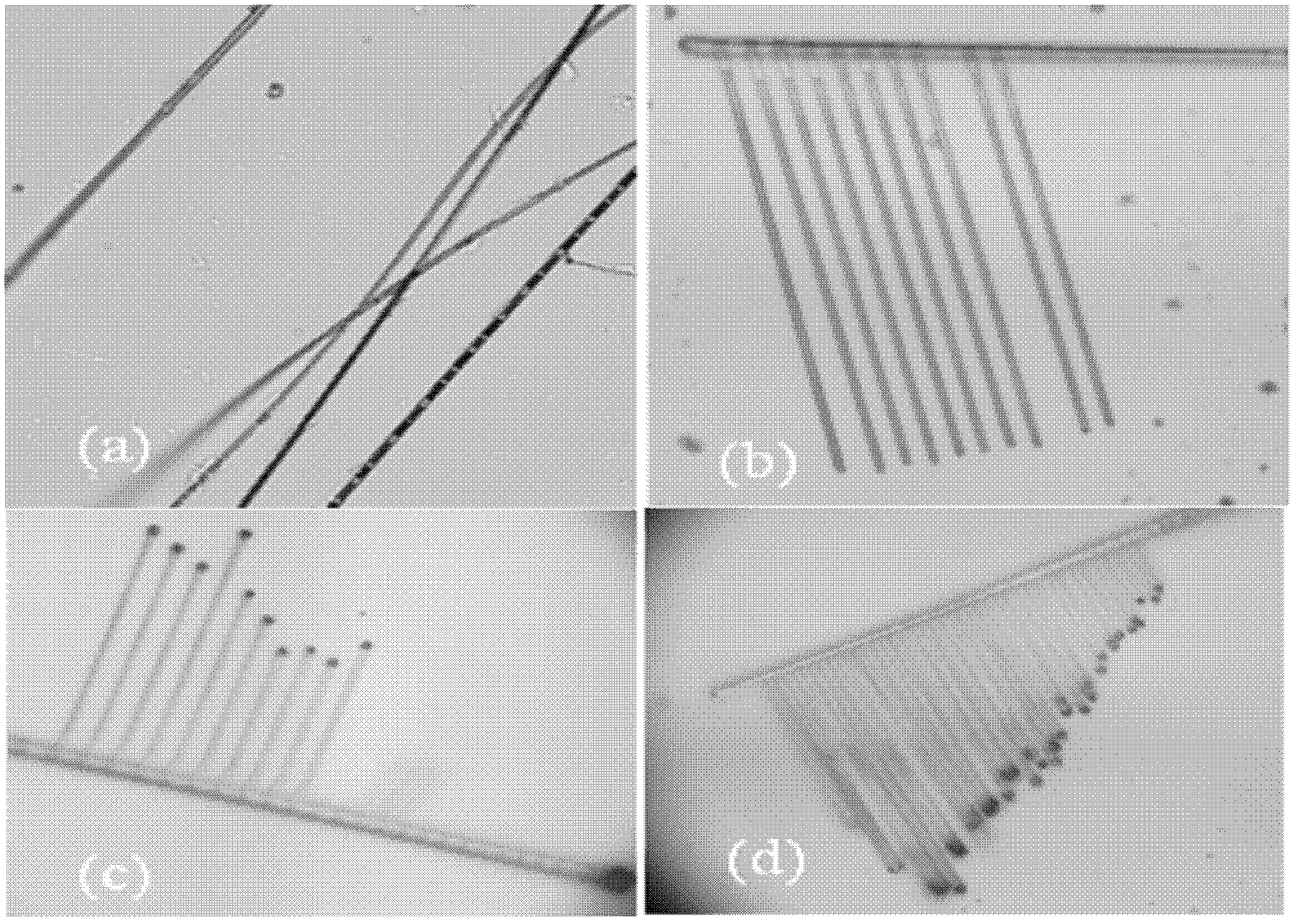
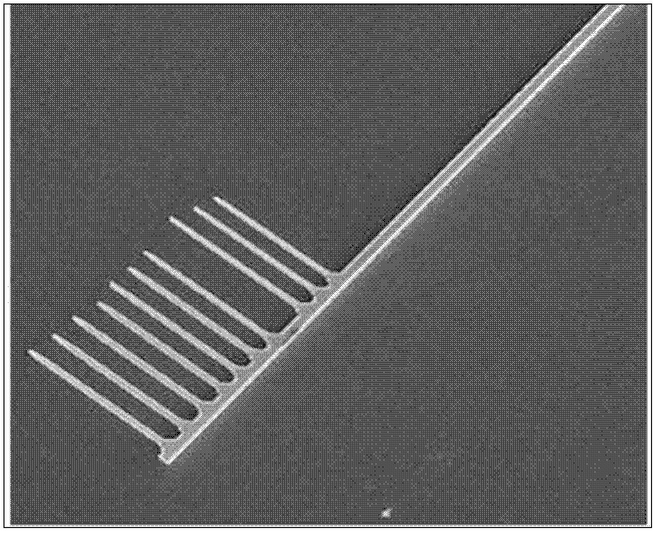
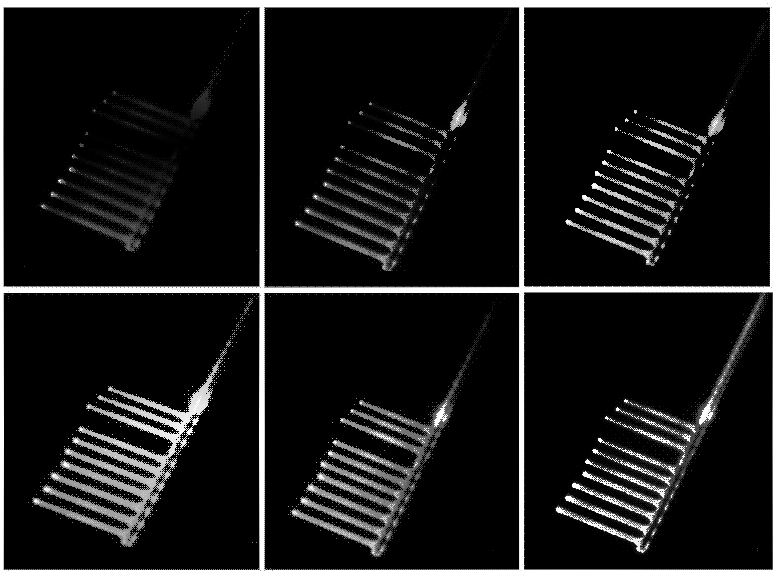
[0027] A cadmium sulfide comb-shaped semiconductor micro-nano material, the material is cadmium sulfide (CdS) doped with tin (Sn), calculated based on the total amount of the material, using transmission electron microscope (TEM) or scanning electron microscope (SEM) The attached energy spectrometer can characterize the molar content of tin within 1%.

[0028] A preparation method of cadmium sulfide comb-shaped semiconductor micro-nano material, the steps are: cadmium sulfide and tin dioxide are uniformly stirred in a mortar at a molar ratio of 100:8 for 10 minutes; silicon wafers are washed in an ultrasonic cleaner with absolute ethanol Clean the inside for 10 minutes. After drying, use the ion sputtering instrument to plate gold for 60 seconds. Clean the porcelain boat and quartz tube for later use. Then put CdS and SnO 2 Put the mixture into the porcelain boat and place the porcelain boat in the center of the quartz tube. Put a gold-plated silicon wafer in another porcelain b...

Embodiment 2

[0030] A preparation method of cadmium sulfide comb-shaped semiconductor micro-nano material. The steps are: cadmium sulfide and tin dioxide are uniformly stirred in a mortar for 10 minutes at a molar ratio of 100:10; silicon wafers are washed in an ultrasonic cleaner with absolute ethanol Clean the inside for 10 minutes. After drying, use the ion sputtering instrument to plate gold for 60 seconds. Clean the porcelain boat and quartz tube for later use. Then put CdS and SnO 2 Put the mixture into the porcelain boat and place the porcelain boat in the center of the quartz tube. Put a gold-plated silicon wafer in another porcelain boat, and place it on the upstream of the quartz tube air flow, 11 cm from the center of the quartz tube. Put the quartz tube into the tube furnace, connect the flow meter upstream of the quartz tube first, connect the exhaust system, connect the exhaust gas treatment system downstream, and then pass in a mixture of argon and hydrogen. After one hour of...

Embodiment 3

[0036] A method for preparing cadmium sulfide comb-shaped semiconductor micro-nano materials, the steps are: cadmium sulfide and tin dioxide are uniformly stirred in a mortar for 10 minutes at a molar ratio of 100:12; silicon wafers are washed in an ultrasonic cleaner with absolute ethanol Clean the inside for 10 minutes. After drying, use the ion sputtering instrument to plate gold for 60 seconds. Clean the porcelain boat and quartz tube for later use. Then put CdS and SnO 2 Put the mixture into the porcelain boat and place the porcelain boat in the center of the quartz tube. Put a gold-plated silicon wafer in another porcelain boat, and place it on the upstream of the quartz tube air flow, 11 cm from the center of the quartz tube. Put the quartz tube into the tube furnace, connect the flow meter upstream of the quartz tube first, connect the exhaust system, connect the exhaust gas treatment system downstream, and then pass in a mixture of argon and hydrogen. After one hour of...


PUM

PropertyMeasurementUnit
diameteraaaaaaaaaa

Abstract

The invention relates to a cadmium sulfide pectinate semiconductor micro / nano material and a preparation method thereof, belonging to the technical field of photochromism. The preparation method comprises the following steps: putting cadmium sulfide and tin dioxide at the center of a quartz pipe of a pipe furnace, putting a gold-plated silicon wafer as a substrate into upstream or downstream the air flow of the quartz pipe of the pipe furnace, introducing carrier gas, heating, keeping the temperature for 1-3 hours, shutting down the pipe furnace, continuing introducing carrier gas, and cooling to room temperature to obtain the tin-doped cadmium sulfide pectinate micro / nano material. The tin-doped cadmium sulfide pectinate micro / nano material has the new application of color variations, and has the characteristics of low cost, simple preparation process and wide raw material sources. Compared with the existing photochromic material, the cadmium sulfide pectinate semiconductor micro / nano material is easier to implement, can implement color variations in real time, and has more color options, so that the photochromic range is more abundant. The invention can be widely applied to the fields of laser display, laser televisions, anti-counterfeiting materials and military wave-absorbing materials.

Description

Technical field [0001] The invention relates to a preparation method of a cadmium sulfide comb-shaped semiconductor micro-nano material, belonging to the technical field of photochromism. Background technique [0002] Every color that appears in the real world, whether it is the color of different lights at night or the colorful billboards we see during the day, has its inherent technical origin and material foundation. The existence of photochromic materials and photochromic technology makes it possible to freely switch various colors, thus making the world we live in more colorful. Generally, photochromism is defined as: under the excitation of an external excitation source, the phenomenon that a substance changes color is called discoloration. Photochromism means that when a compound A is irradiated with light of a certain wavelength, it can undergo a photochemical reaction to obtain product B. The colors of A and B (that is, the absorption of light) are significantly differe...

Claims


Application Information

Patent Timeline
Patent Type & Authority Patents(China)
IPC IPC(8): C01G11/02B82Y40/00
Inventor 刘瑞斌邹炳锁张春花
Owner BEIJING INSTITUTE OF TECHNOLOGYGY
Why Eureka
Try Eureka