Atomic layer deposition device

A technology of atomic layer deposition and electrode, which is applied in the direction of coating, metal material coating process, gaseous chemical plating, etc., can solve the problems of low plasma density, deposition rate, deposition film quality, etc.

Active Publication Date: 2012-09-19
BEIJING INSTITUTE OF GRAPHIC COMMUNICATION
View PDF2 Cites 20 Cited by
  • Summary
  • Abstract
  • Description
  • Claims
  • Application Information

AI Technical Summary

Problems solved by technology

[0005] However, in the prior art, there is a common problem that the plasma density in the plasma region

Method used


Image

  • Atomic layer deposition device
  • Atomic layer deposition device
  • Atomic layer deposition device

Examples


Embodiment Construction

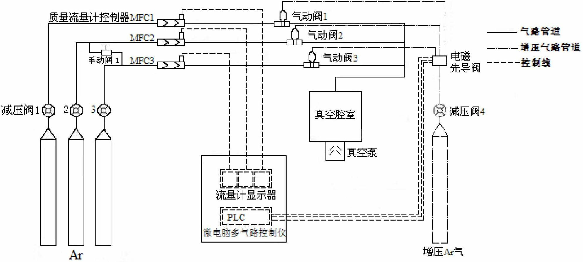
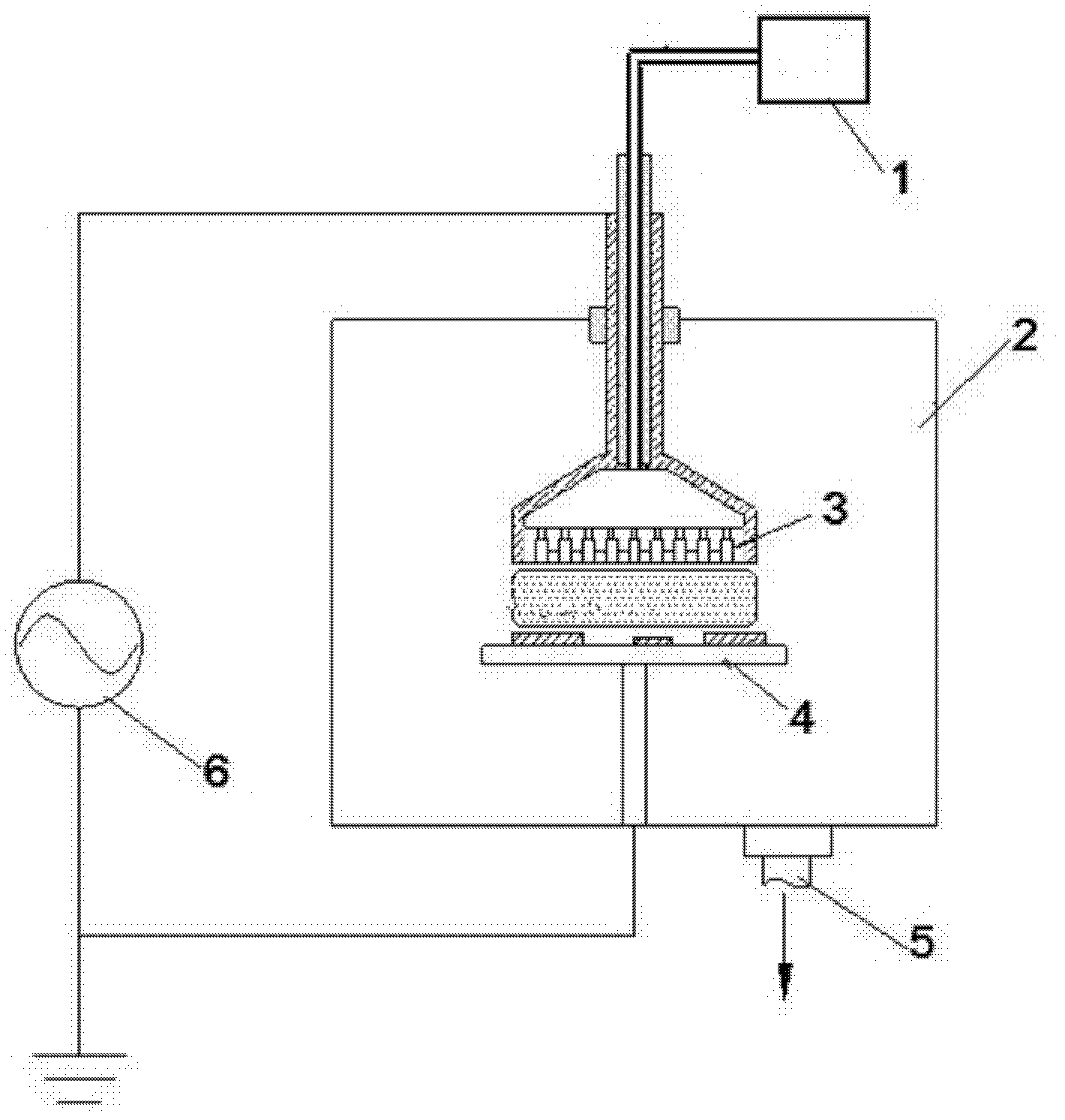
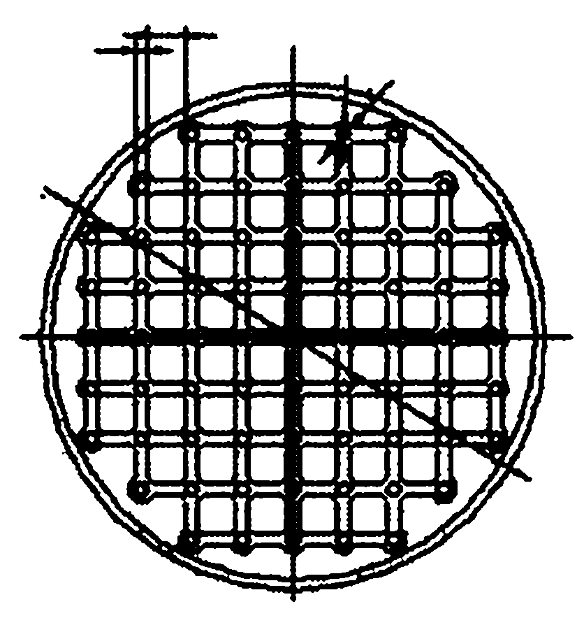
[0027] The invention provides an atomic layer deposition device with an arrayed hollow cathode structure. The set of devices includes a gas distribution system 1, a vacuum chamber 2, an array type hollow electrode 3, a flat plate electrode 4, a vacuum system 5, and a power supply system 6, etc. Utilizing the hollow cathode discharge effect of the arrayed hollow electrodes 3, the ionization efficiency of the gas can be greatly improved, the pressure and plasma density of the discharge gas can be increased, and the activation efficiency of the reaction monomer in the atomic layer deposition process can be improved, and the ionization efficiency in the space can be increased. The concentration of active groups can greatly increase the deposition rate of the film and reduce the deposition temperature. The measurement results show that this array type hollow discharge can increase the plasma density to 10 11 ~10 13 / cm 3 , reduce the plasma energy below 1eV, increase the deposit...


PUM


Abstract

The invention discloses an atomic layer deposition device, belongs to the technical field of plasma application, and relates to a plasma generator with an array hollow cathode structure. The device comprises a gas distribution system (1), a vacuum chamber (2), an array hollow cathode upper electrode (3), a flat plate grounding lower electrode (4), a vacuum-pumping system (5) and a power system (6), wherein the array hollow cathode upper electrode (3) is provided with a plurality of uniformly distributed through holes with diameter ranging from 1 to 3 mm, and a space between adjacent through holes is 2-4mm; a space between the array hollow cathode upper electrode (3) and the flat plate grounding lower electrode (4) is 5-20mm; and the array hollow cathode upper electrode (3) is connected with a gas supply pipeline of the gas distribution system (1). By the device, the plasma temperature is reduced, and other plasma parameters are improved, so that the deposition efficiency is improved and the microstructure and performance of the deposited material are optimized.

Description

Technical field: [0001] The invention belongs to the field of plasma application technology and relates to a plasma generator with an array type hollow cathode structure. The device combines the atomic layer deposition function with the hollow cathode discharge feature. The hollow cathode electrode structure can increase the plasma density during discharge, reduce the plasma temperature, and improve some other plasma parameters, thereby increasing the deposition efficiency and optimizing the plasma. Microstructure and properties of deposited materials. Background technique: [0002] Atomic layer deposition (ALD, Atomic Layer Deposition) is an improved chemical vapor deposition technique, originally called atomic layer epitaxy. It was first invented by Finns Suntola T and Antson M J, so they also applied for patent protection in 1977, but they did not receive much attention at first. It was not until the 1990s that atomic-layer technology developed significantly due to the ...

Claims


Application Information

Patent Timeline
IPC IPC(8): C23C16/50
Inventor 陈强杨丽珍王正铎桑利军刘忠伟张受业
Owner BEIJING INSTITUTE OF GRAPHIC COMMUNICATION
Why Eureka
Try Eureka