Preparation method of yttrium aluminum oxygen composite oxide high K medium thin film transistor

A composite oxide and dielectric thin film technology, applied in semiconductor/solid-state device manufacturing, electrical components, circuits, etc., can solve the problems of small forbidden band width, hinder the development of TFT, and small relative dielectric constant, and achieve dense and simplified thin films. The effect of simple process and preparation process

Inactive Publication Date: 2012-09-19
NINGBO INST OF MATERIALS TECH & ENG CHINESE ACADEMY OF SCI
View PDF5 Cites 14 Cited by
  • Summary
  • Abstract
  • Description
  • Claims
  • Application Information

AI Technical Summary

Problems solved by technology

At present, the gate dielectric with mature technology and large-scale application is SiO 2 , but it has disadvantages that hinder the further development of TFT: small forbidden band width (Eg=3.9), small relative permittivity (εr=1.45)

Method used


Image

  • Preparation method of yttrium aluminum oxygen composite oxide high K medium thin film transistor
  • Preparation method of yttrium aluminum oxygen composite oxide high K medium thin film transistor
  • Preparation method of yttrium aluminum oxygen composite oxide high K medium thin film transistor

Examples


Embodiment 1

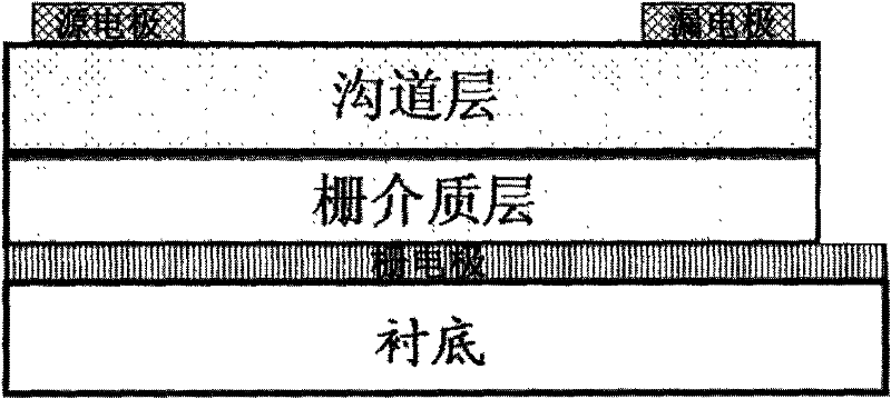
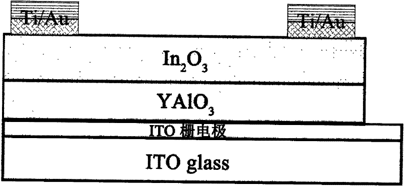
[0032] A YAlO with Bottom Gate Structure 3 A method for preparing a composite oxide high-K dielectric thin film transistor, the specific process is:

[0033] Step 1: Select commercially purchased ITO glass as the substrate, and leave a part of the edge of the glass as the gate electrode during preparation. The surface resistivity of the ITO glass is less than 15Ω / cm 2 ;

[0034] Step 2: Use magnetron sputtering equipment and metal yttrium target (Y) and aluminum target (Al), and react with oxygen at room temperature to sputter and deposit YAlO with a thickness of about 150nm 3 composite oxide dielectric film, then in O 2 Perform rapid annealing treatment under atmosphere, the annealing temperature is 200°C to 400°C, the heating rate is 20°C / min, and the annealing time is 10min;

[0035] Step 3: Using the method of magnetron sputtering, in O 2 Deposition of In at room temperature under atmosphere 2 o3 channel layer;

[0036] Step 4: Prepare Ti / Au source electrode and drai...

Embodiment 2

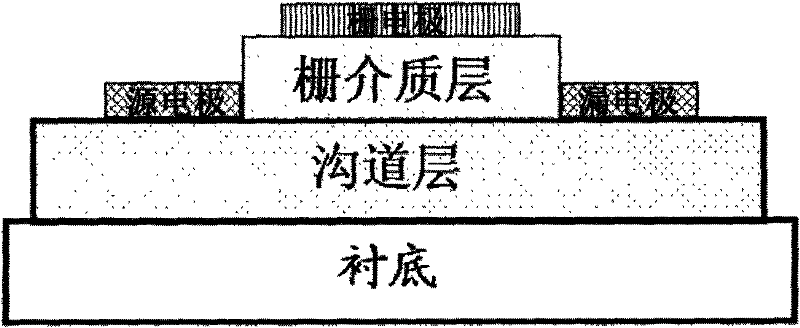
[0038] YAlO with a top-gate structure 3 A method for preparing a composite oxide high-K dielectric thin film transistor, the specific process is:

[0039] Step 1: Select commercially purchased ITO glass as the substrate, and the surface resistivity of the ITO glass is less than 15Ω / cm 2 ;

[0040] Step 2: Using the method of magnetron sputtering, in O 2 Deposition of In on ITO glass at room temperature under atmosphere 2 o 3 channel layer;

[0041] Step 3: Using magnetron sputtering equipment with metal yttrium target (Y) and aluminum target (Al), at room temperature on In 2 o 3 About 150nm YAlO was deposited on the channel layer by co-reactive sputtering with oxygen 3 composite oxide dielectric film, then in O 2 Perform rapid annealing treatment under atmosphere, the annealing temperature is 200°C to 400°C, the heating rate is 20°C / min, and the annealing time is 10min;

[0042] Step 4: Use electron beam evaporation equipment and Al mask to prepare Ti / Au source electr...

Embodiment 3

[0044] A YAlO with Bottom Gate Structure 3 A method for preparing a composite oxide high-K dielectric thin film transistor, the specific process is:

[0045] Step 1: Select commercially purchased ITO glass as the substrate, and leave a part of the edge of the glass as the gate electrode during preparation. The surface resistivity of the ITO glass is less than 15Ω / cm 2 ; and the substrate temperature is heated to 250°C.

[0046] Step 2: Use magnetron sputtering equipment, metal yttrium target (Y) and aluminum target (Al), and react with oxygen to sputter and deposit about 150nm YAlO under substrate temperature conditions 3 composite oxide dielectric film, then in O 2 Perform rapid annealing treatment under atmosphere, the annealing temperature is 200°C to 400°C, the heating rate is 20°C / min, and the annealing time is 10min;

[0047] Step 3: Using the method of magnetron sputtering, in O 2 Depositing In at atmospheric substrate temperature 2 o 3 channel layer;

[0048] St...


PUM

PropertyMeasurementUnit
thicknessaaaaaaaaaa

Abstract

The invention discloses a preparation method of a YAIO3 composite oxide high K medium thin film transistor, which comprises the following steps of: taking a metal yttrium target (Y) and an aluminum target (A1) as source materials, preparing a gate dielectric layer material of a YAIO3 composite oxide high K medium as the thin film transistor by adopting a magnetron sputtering and rapid annealing technology, taking ITO (Indium Tin Oxide) glass as a substrate and taking source and drain electrodes as Ti / Au double-layered metal film electrodes; and the prepared thin film transistor can adopt a top gate structure or a bottom gate structure. The preparation method is simple and controllable, the low-temperature preparation can be realized, and the manufacturing cost is lower; and the prepared thin film transistor is excellent in performance, has smaller leakage current and larger capacitor, can be developed into a full-transparent thin film transistor and has very wide application prospect in the technical field of display devices.

Description

technical field [0001] The invention relates to the technical field of preparation of thin film transistors, in particular to a yttrium aluminum oxide (YAlO 3 ) A method for preparing a composite oxide high-K dielectric thin film transistor. Background technique [0002] Thin-film transistors (TFTs) generally consist of a substrate, a gate dielectric layer, a channel layer, a gate electrode, and source-drain electrodes, including TFTs with a bottom-gate structure (such as figure 1 shown) and TFT with top gate structure (such as figure 2 shown). TFTs are mainly used as switching elements for driving pixels in display devices such as liquid crystal displays (TFT-LCDs). Among them, the bandgap width of the gate dielectric material determines the size of the TFT leakage current, and its relative permittivity determines the size of the subthreshold swing of the device (Thin Solid Films 517, 4115, 2009), that is, the size of the energy consumption , so the gate dielectric lay...

Claims


Application Information

Patent Timeline
Patent Type & Authority Applications(China)
IPC IPC(8): H01L21/336H01L21/203
Inventor 俞峥曹鸿涛梁凌燕许望颖方燕群叶小娟
Owner NINGBO INST OF MATERIALS TECH & ENG CHINESE ACADEMY OF SCI
Why Eureka
Try Eureka