Method for cleaning waste silicon material generated in silicon wafer treatment process

A processing process and technology of silicon material, which is applied in the direction of final product manufacturing, sustainable manufacturing/processing, electrical components, etc., can solve the problems of incomplete cleaning of waste silicon material, low work efficiency, etc., so as to improve work efficiency and save costs. Effect

Inactive Publication Date: 2012-09-26
保定晶创硅材料制造有限公司
View PDF3 Cites 15 Cited by
  • Summary
  • Abstract
  • Description
  • Claims
  • Application Information

AI Technical Summary

Problems solved by technology

[0004] The purpose of the present invention is to provide a method for cleaning waste silicon produced during the processing of sil

Method used


Image

  • Method for cleaning waste silicon material generated in silicon wafer treatment process
  • Method for cleaning waste silicon material generated in silicon wafer treatment process

Examples


Embodiment 1

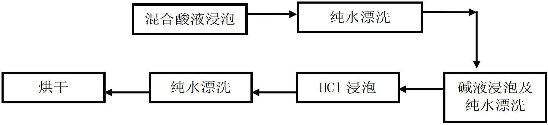
[0026] The specific process is as figure 1 Shown:

[0027] 1) Soak the waste silicon material in a mixed acid solution with a mass percentage of 5% for 15 minutes, then put the waste silicon material into circulating pure water with a conductivity of 14-16 trillion and rinse it with ultrasonic waves for 15 minutes; 2) Soak the waste silicon material soaked in the mixed acid solution in 15wt% NaOH solution, soak for 5 minutes at 80°C, and then put the waste silicon material into circulating pure water with a conductivity of 14~16M and use ultrasonic waves Rinse for 5 minutes; 3) Soak the waste silicon material in 5wt% HCl solution for 10 minutes, then rinse with pure water and dry, wherein the mixed acid solution is the acid solution discarded during the battery preparation process.

[0028] After inspection, the impurities and oxide layer on the waste silicon material were cleaned, and the surface loss was controlled at 10-20 microns.

Embodiment 2

[0030] 1) Soak the waste silicon material in a mixed acid solution with a mass percentage of 5% for 10 minutes, then put the waste silicon material into circulating pure water with a conductivity of 14-16 trillion and rinse it with ultrasonic waves for 10 minutes; 2) Soak the waste silicon material soaked in the mixed acid solution in 25wt% NaOH solution, soak for 10 minutes at 80°C, and then put the waste silicon material into circulating pure water with a conductivity of 14-16 megabytes for ultrasonic treatment. Rinse for 10 minutes; 4) Soak the waste silicon material in 15wt% HCl solution for 5 minutes, then rinse with pure water and dry, wherein the mixed acid solution is the acid solution discarded during the battery preparation process.

[0031] After inspection, the impurities and oxide layer on the waste silicon material were cleaned, and the surface loss was controlled at 10-20 microns.

[0032] In summary, the present invention can reduce the labor intensity of worke...


PUM


Abstract

The invention discloses a method for cleaning a waste silicon material generated in a silicon wafer treatment process, which comprises the following steps: 1) soaking the waste silicon material to be washed in a mixed acid liquid, and rinsing with pure water; 2) soaking the waste silicon material subjected to mixed acid liquid soaking in an alkali liquid, and rinsing with pure water; and 3) soaking the waste silicon material in a hydrochloric acid solution, rinsing with pure water, and drying, wherein the mixed acid liquid is the waste acid liquid generated in the battery preparation process. According to the technical scheme, the invention can effectively and thoroughly eliminate the surface and embedded impurities of the waste silicon material without causing silicon material loss; and since most impurities are removed by acid erosion or alkali erosion instead of manual sanding, the work efficiency is enhanced. Besides, the mixed acid liquid is the waste acid liquid in the battery preparation process, thereby saving the cost and making contributions to wastewater treatment, emission reduction and consumption reduction.

Description

technical field [0001] The invention relates to the technical field of solar cell processing, in particular to a method for cleaning waste silicon material generated during the processing of silicon wafers. Background technique [0002] In the process of producing solar monocrystalline polycrystalline silicon wafers, redundant head and tail skins and residues after cutting will be generated. Impurities such as cutting fluid, metal ions, and accompanying silica gel remain on the surface during processing. If you want to reuse these silicon materials, you must do cleaning. [0003] At present, the commonly used cleaning method in the photovoltaic industry is manual sandblasting and grinding, that is, operators operate sandblasting machine tools to remove visible impurities mechanically. This cleaning method is not easy to deal with deeply embedded silicon carbide, and the cutting loss is large. If there are many impurities on the surface of the silicon block, it will not onl...

Claims


Application Information

Patent Timeline
IPC IPC(8): H01L31/18
CPCY02P70/50
Inventor 冯文宏刘俊飞
Owner 保定晶创硅材料制造有限公司
Why Eureka
Try Eureka