

Bonding method for light-emitting diode (LED) chip and LED chip
A LED chip and bonding technology, applied in the direction of welding media, electrical components, welding/cutting media/materials, etc., can solve the problems of narrow process window and high manufacturing cost, achieve the best bond and interface, reduce the use of precious metals, reduce The effect of manufacturing costs
- Summary
- Abstract
- Description
- Claims
- Application Information
AI Technical Summary
Problems solved by technology
Method used
Image

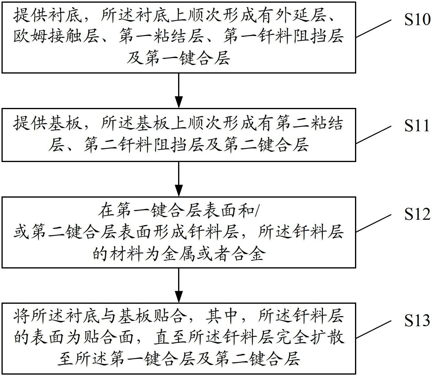
Examples
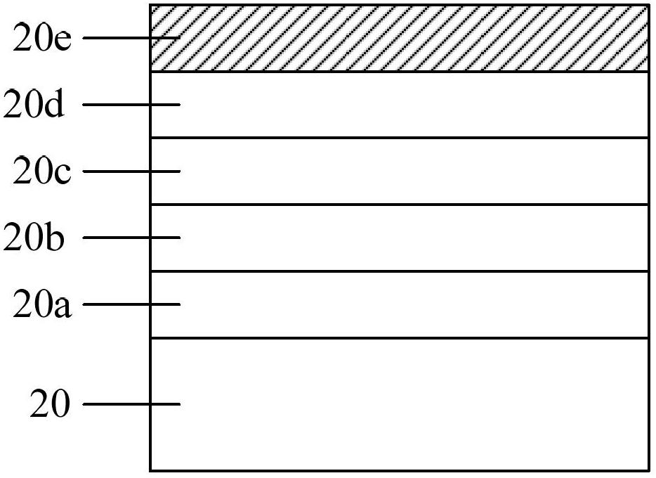
Embodiment 1
[0050] Please refer to Figure 2a~2e , Which is a schematic cross-sectional view of the device in the LED chip bonding method of the first embodiment of the present invention.
[0051] First, like Figure 2a As shown, a substrate 20 is provided on which an epitaxial layer 20a, an ohmic contact layer 20b, a first adhesive layer 20c, a first solder barrier layer 20d, and a first bonding layer 20e are sequentially formed on the substrate 20. Preferably, the material of the substrate 20 is GaN, the epitaxial layer 20a is a GaN-based epitaxial layer, and the epitaxial layer 20a is formed by an epitaxial process. In other embodiments of the present invention, the material of the substrate 20 may also be silicon, silicon carbide, GaAs, AlN or ZnO.
[0052] In this embodiment, the material of the first adhesive layer 20c is Ti, and the thickness thereof is 30 nm to 70 nm. Preferably, the thickness of the first adhesive layer 20c is 50 nm. The material of the first solder barrier layer 20d...
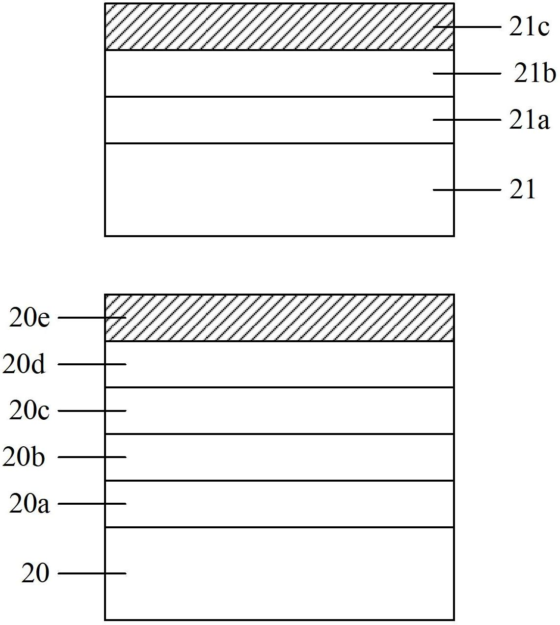
Embodiment 2
[0069] Please refer to image 3 , Which is a schematic cross-sectional view of the device in the LED chip bonding method of the second embodiment of the present invention.
[0070] Such as image 3 As shown, in this embodiment, a substrate 30 is provided, and an epitaxial layer 30a, an ohmic contact layer 30b, a mirror layer 30c, a mirror barrier layer 30d, and a first adhesive layer 30e are sequentially formed on the substrate 30. , The first solder barrier layer 30f and the first bonding layer 30g. Wherein, the material of the first bonding layer 30e is Ti, and its thickness is preferably 50nm; the material of the first brazing filler metal barrier layer 30f is TiW, and the thickness is preferably 200nm; the thickness of the first bonding layer 30g The material is Ni, and its thickness is preferably 1 micron.
[0071] Please continue to refer image 3 , A substrate 31 is provided on which a second adhesive layer 31a, a second solder barrier layer 31b, a second bonding layer 31c,...
Embodiment 3
[0076] Please refer to Figure 4 , Which is a schematic cross-sectional view of the device in the LED chip bonding method of the third embodiment of the present invention.
[0077] Such as Figure 4 As shown, in this embodiment, a substrate 40 is provided, and an epitaxial layer 40a, an ohmic contact layer 40b, a mirror layer 40c, a mirror barrier layer 40d, and a first bonding layer 40e are sequentially formed on the substrate 40. , The first solder barrier layer 40f, the first bonding layer 40g, and the first solder layer 42. Wherein, the material of the first bonding layer 40e is Ti, and its thickness is preferably 50nm; the material of the first brazing filler metal barrier layer 40f is TiW, and the thickness is preferably 200nm; the thickness of the first bonding layer 40g The material is Ni, and its thickness is preferably 1 micron; the material of the first solder layer 42 is Sn x Cu 1-x , The thickness is preferably 250 nm.
[0078] Please continue to refer Figure 4 , A s...
PUM
| Property | Measurement | Unit |
|---|---|---|
| melting point | aaaaa | aaaaa |
| thickness | aaaaa | aaaaa |
| thickness | aaaaa | aaaaa |
Abstract
Description
Claims
Application Information