
Manufacturing method for light emitting diode (LED) metal base board

A technology for light-emitting diodes and metal substrates, which is applied to electrical components, circuits, semiconductor devices, etc., can solve the problems of difficult splintering of metal substrates, difficult processes, weak bonding strength, etc., to meet large-scale industrial production, and the process method is simple and reliable. , the effect of cheap and easy-to-obtain raw materials

Inactive Publication Date: 2012-10-03
TONGFANG OPTO ELECTRONICS
View PDF5 Cites 2 Cited by
  • Summary
  • Abstract
  • Description
  • Claims
  • Application Information

AI Technical Summary

Problems solved by technology

Although the electroplating method has many advantages, it also has its inherent disadvantages, especially the substrate obtained by electroplating, its bonding strength with the GaN epitaxial layer is weak, and metal chips are easy to adhere to the grinding wheel or cutter during mechanical cutting. The good thermal conductivity of the metal itself leads to thermal damage to the core particles, making it difficult for the metal substrate to be split, resulting in difficulties in subsequent processes

Method used


Image

  • Manufacturing method for light emitting diode (LED) metal base board
  • Manufacturing method for light emitting diode (LED) metal base board
  • Manufacturing method for light emitting diode (LED) metal base board

Examples


Embodiment Construction

[0022] Method steps of the present invention are as follows:

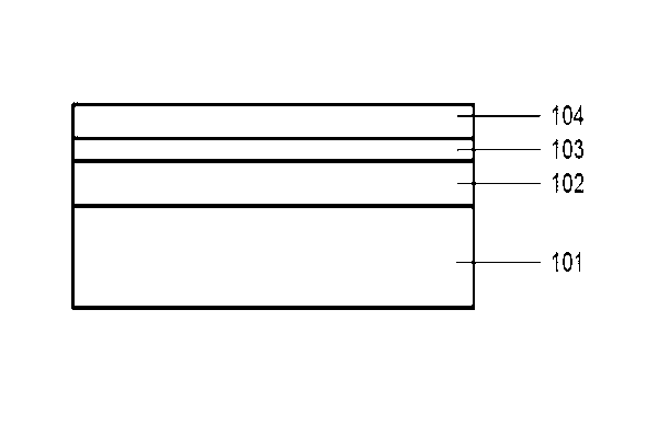
[0023] see figure 1 , growing an N-type GaN-based semiconductor layer 102, a quantum well active region 103, and a P-type GaN-based semiconductor layer 104 sequentially on a sapphire substrate 101 by metal-organic chemical vapor deposition;

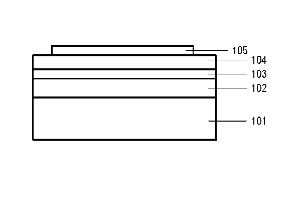
[0024] see figure 2 , on the P-type GaN-based semiconductor layer 104, vapor-deposit a metal layer reflector 105 with a thickness of 1000-10000 Å; anneal at a high temperature for 10-30min in a nitrogen atmosphere to form a gap between the metal reflective layer 105 and the P-type GaN-based semiconductor layer 104 Ohmic contact, and enhance the bonding force between the two;

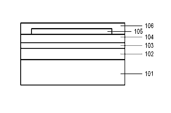
[0025] see image 3 , sputtering one or more layers of metal on the metal reflective layer 105 and the P-type GaN-based semiconductor layer 104 as the seed layer 106; using photolithography and wet chemical etching to form the seed layer 106 on the position that will need splits in the future ...


PUM

PropertyMeasurementUnit
thicknessaaaaaaaaaa

Abstract

The invention discloses a manufacturing method for a light emitting diode (LED) metal base board, which relates to a substrate transition technology in the technical field of photoelectricity. The method comprises the following steps of: sequentially growing an N-typed GaN semi-conductive layer, a quantum well active layer and a P-typed GaN semi-conductive layer on a sapphire substrate; carrying out vapor depositing on a metal mirror reflective layer on the P-typed GaN semi-conductive layer; pre-plating multiple metal layers as a seed layer on a face of an appliance which needs a substrate transition through the electroplating; coating with photoresist on a channel; carrying out oxidization on the metal surface of the seed layer, and the metal base board is obtained through the method of electroplating; and cutting along the position of photoresist to obtain the required core particles. According to the manufacturing method, the combination strength of the metal base board and a GaN extension layer is high, and convenience in mechanical cutting can be easily realized, the manufacturing method has the advantages of simple process, low cost and easiness in obtaining raw materials.

Description

technical field [0001] The invention relates to a substrate transfer technology in the field of photoelectric technology, in particular to a method for manufacturing a metal substrate in a GaN-based light-emitting diode with a high-power vertical structure. Background technique [0002] The birth of semiconductor lighting sources is hailed as another revolution in the field of lighting, and it is attracting more and more people to carry out continuous research and development on it. In order to make light-emitting diode LED enter the general lighting market with extremely broad prospects from the currently widely used special lighting such as signal lights and rear projections, it is necessary to vigorously develop white LEDs. Therefore, it is not only necessary to improve the luminous efficiency of GaN-based LED devices, but also to prepare LEDs that can withstand high current density and high power structures. At present, because the vertical structure LED can avoid the ...

Claims


Application Information

Patent Timeline
Patent Type & Authority Applications(China)
IPC IPC(8): H01L33/00H01L33/02H01L33/32
Inventor 张华东康学军郭德博刘刚
Owner TONGFANG OPTO ELECTRONICS
Learn More