Ultraviolet light-emitting diode chip with reflection ohmic contact electrode

A technology for ohmic contact electrodes and light-emitting diodes, which is applied in circuits, electrical components, semiconductor devices, etc., can solve the problems of difficult to obtain ohmic contact between aluminum and P-type layers.

Inactive Publication Date: 2012-10-03
INST OF SEMICONDUCTORS - CHINESE ACAD OF SCI
View PDF5 Cites 8 Cited by
  • Summary
  • Abstract
  • Description
  • Claims
  • Application Information

AI Technical Summary

Problems solved by technology

Although the reflectivity of aluminum in the ultraviolet band is high, because the work function of the P-type layer is high (7.5eV)

Method used


Image

  • Ultraviolet light-emitting diode chip with reflection ohmic contact electrode
  • Ultraviolet light-emitting diode chip with reflection ohmic contact electrode

Examples


Embodiment Construction

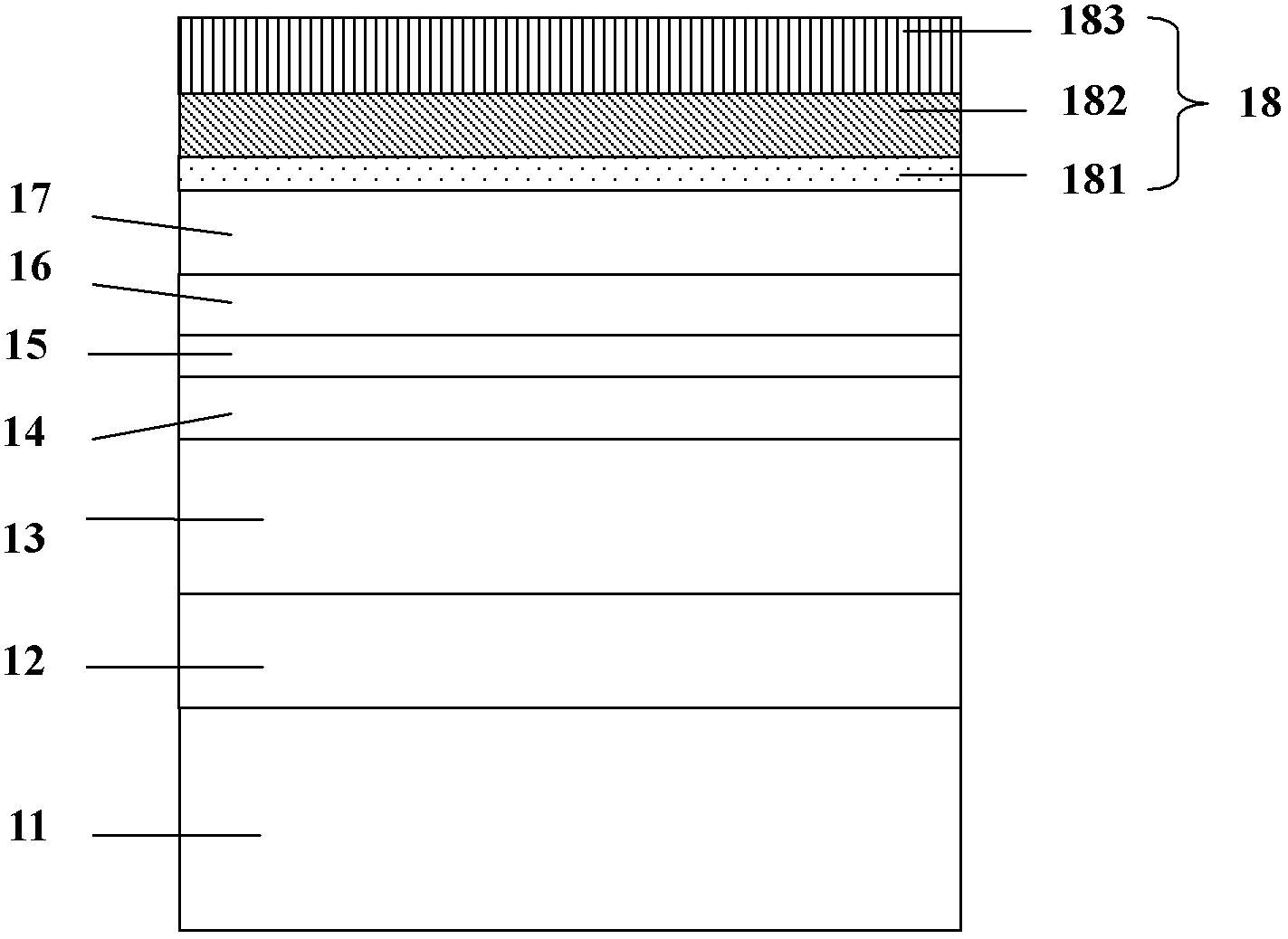
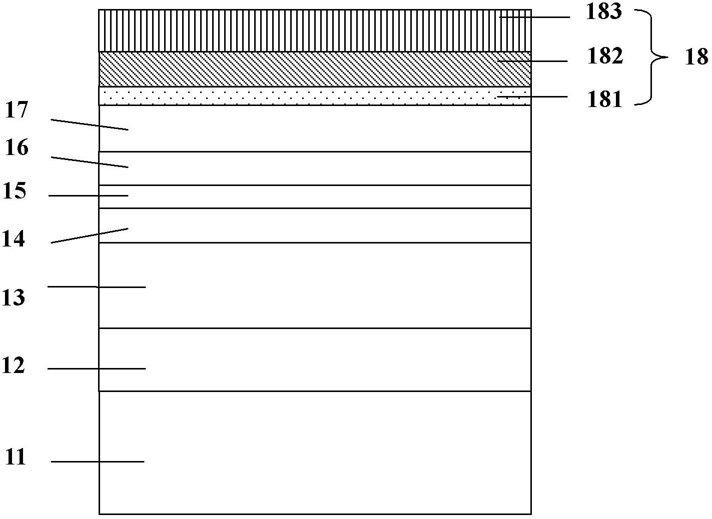
[0016] Please refer to figure 1 Shown, a kind of substrate of the ultraviolet light-emitting diode with reflective ohmic contact electrode of the present invention comprises:

[0017] A substrate 11, the material of the substrate 11 is sapphire or AlN;

[0018] An AlN template layer 12, which is grown on the substrate 11 by metal organic compound vapor deposition (MOCVD), and has a thickness of 0.1-10 μm;

[0019] An N-type AlGaN layer 13, grown on the AlN template layer 12 by MOCVD, with a thickness of 1-5 μm;

[0020] An active region 14 of multiple quantum wells, which is grown on the N-type AlGaN layer 13 by MOCVD, and its material is Al x Ga 1-x N / Al y Ga 1-y N-based materials, where 0≤x

[0021] An electron blocking layer 15, which is grown on the active region 14 of the multi-quantum well by MOCVD method, and its material is an AlGaN material with a high Al composition, and its Al composition is higher than that of the multi-quantum well active region 14, and...


PUM

PropertyMeasurementUnit
Thicknessaaaaaaaaaa
Thicknessaaaaaaaaaa
Thicknessaaaaaaaaaa

Abstract

The invention relates to an ultraviolet light-emitting diode chip with a reflection ohmic contact electrode. The ultraviolet light-emitting diode chip comprises a substrate, an AlN template layer, an N-type AlGaN layer, a multiquantum-well active region, an electronic barrier layer, a P-type transition layer, a P-type contact layer and the reflection ohmic contact electrode, wherein the AlN template layer grows on the substrate; the N-type AlGaN layer grows on the AlN template layer; the multiquantum-well active region grows on the N-type AlGaN layer; the electronic barrier layer grows on the multiquantum-well active region; the P-type transition layer grows on the electronic barrier layer; the P-type contact layer grows on the P-type transition layer; and the reflection ohmic contact electrode is made on the P-type contact layer. An ultraviolet light-emitting diode prepared from the chip has the light emitting wavelength range of 200nm to 365nm. The chip has high ultraviolet reflectivity, so that the light extraction efficiency of the ultraviolet light-emitting diode is improved.

Description

technical field [0001] The invention belongs to the technical field of semiconductors, in particular to a substrate of an ultraviolet light-emitting diode with reflective ohmic contact electrodes. The invention can effectively improve the light extraction efficiency of the ultraviolet light-emitting diode, and has good ohmic contact performance. Background technique [0002] At present, ultraviolet (200nm-365nm) light-emitting diodes adopt a flip-chip, thin film flip-chip or vertical structure, that is, the ultraviolet light emitted from the quantum well is emitted from the sapphire or N-type layer. Side launch out. Due to the strong absorption of ultraviolet light (200nm-365nm) and low reflectivity of the P-type layer and the P-electrode, the light radiated from the quantum well to the P-type layer is absorbed by the P-type layer and the electrode above it, thus Can not be extracted, resulting in lower light extraction efficiency and serious loss of light radiation power....

Claims


Application Information

Patent Timeline
IPC IPC(8): H01L33/36H01L33/40
Inventor 董鹏闫建昌王军喜孙莉莉曾建平丛培沛李晋闽
Owner INST OF SEMICONDUCTORS - CHINESE ACAD OF SCI
Why Eureka
Try Eureka