
CMOS (complementary metal-oxide-semiconductor transistor) image sensor for realizing two-dimensional discrete cosine transformation

A two-dimensional discrete cosine, image sensor technology, applied in image communication, color TV parts, TV system parts and other directions, can solve the problem of low acquisition and processing efficiency, increase image sensor power consumption and chip area, restrict image sensor application and other issues to achieve the effect of shortening computing time, reducing parts, and reducing power consumption

Inactive Publication Date: 2012-10-03
TIANJIN UNIV
View PDF3 Cites 13 Cited by
  • Summary
  • Abstract
  • Description
  • Claims
  • Application Information

AI Technical Summary

Problems solved by technology

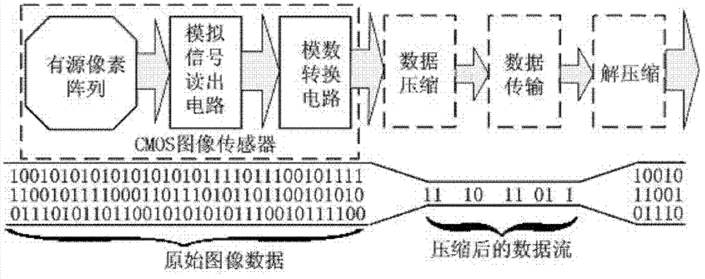
However, the process itself has the problem of low collection and processing efficiency: the front-end CIS collects and processes the complete image information and consumes a lot of power consumption and processing power, and the large amount of redundant information contained in the output data is in the process of data compression. In the end, only part of the information is stored and transmitted, and the operation of image acquisition and data compression on redundant information is actually doing useless work
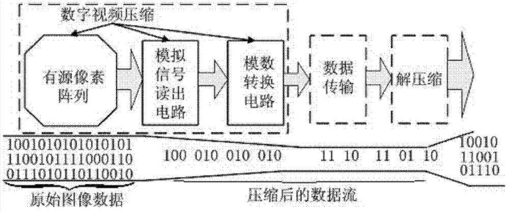
DSP can increase the speed and precision of signal processing, but it increases the power consumption and chip area of ​​image sensors, which seriously restricts the application of image sensors in wireless sensing, biomedical and other fields. These fields need to obtain a large amount of image information and timely Compress it, etc., without increasing power consumption and area

Method used


Image

  • CMOS (complementary metal-oxide-semiconductor transistor) image sensor for realizing two-dimensional discrete cosine transformation
  • CMOS (complementary metal-oxide-semiconductor transistor) image sensor for realizing two-dimensional discrete cosine transformation
  • CMOS (complementary metal-oxide-semiconductor transistor) image sensor for realizing two-dimensional discrete cosine transformation

Examples


Embodiment Construction

[0031]The traditional CMOS image sensor array architecture includes a pixel array for receiving light signals and converting them into voltage signals, amplifying the voltage signals and performing correlated double sampling (CDS) to eliminate fixed pattern noise (FPN) and reset noise readout circuit, a multiplexer (MUX) for selecting specific pixel values ​​for subsequent amplification, a programmable gain amplifier (DPGA) for amplifying voltage signals corresponding to pixel values ​​for analog-to-digital conversion, and converting voltage values ​​into digital The signal is processed by an analog-to-digital converter (ADC) for subsequent digital image processing and peripheral control timing circuits. This invention will improve the traditional CMOS image sensor architecture and realize 2D-DCT by mixed signal processing.

[0032] Suppose {X(m, n)|m=0, 1,..., M-1; n=0, 1,..., N-1} is a two-dimensional image signal data matrix, and its two-dimensional discrete cosine Transfo...


PUM


Abstract

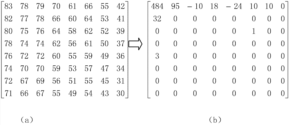
The invention relates to the field of the integrated circuit design of micro-electronics and the field of encoding and compressing of a digital image. A CMOS (complementary metal-oxide-semiconductor transistor) image sensor structure for realizing 2D-DCT (two-dimensional-discrete cosine transformation) is provided so that the 2D-DCT is finished in a process of obtaining an image; and compared with the traditional processing flow, the area and power consumption for introducing a 2D-DCT module which is extra used are reduced on the basis of not reducing the sensing quality of the image. The technical scheme disclosed by the invention is as follows: the CMOS image sensor for realizing the two-dimensional discrete cosine transformation comprises a pixel array, a read-out circuit, a switch capacitance array, a multi-path selector MUX (multiplexer), a DPGA (digital programmable gain amplifier), an ADC (analogue-to-digital converter) and a control time sequence circuit and further comprises an analogue accumulator; and the ADC is internally and additionally provided with a switch control module 2, a register 2, a capacitance access and a digital accumulator. The CMOS image sensor disclosed by the invention is mainly applied to encoding and compressing the image sensor.

Description

technical field [0001] The present invention relates to the field of integrated circuit design of microelectronics and the field of digital image coding compression, especially a switched capacitor amplifier circuit, an analog accumulator and a two-dimensional discrete cosine transform (Two-Dimensional Discrete Cosine Transform, 2D-DCT), specifically, It relates to a CMOS image sensor that realizes two-dimensional discrete cosine transform. Background technique [0002] The CMOS image sensor (CMOS Image Sensor, CIS) based on the standard CMOS process has gradually become the mainstream device for image and video acquisition due to its characteristics of monolithic integration, low power consumption, low cost, small size, and image information can be read randomly. . [0003] The traditional CIS-based video signal acquisition and processing process mainly includes four parts: image acquisition, data compression, data transmission and decompression, such as figure 1 shown. ...

Claims


Application Information

Patent Timeline
Patent Type & Authority Applications(China)
IPC IPC(8): H04N5/3745H04N5/378H04N5/341
Inventor 姚素英王龙菲徐江涛高静史再峰李渊清李毅强
Owner TIANJIN UNIV
Learn More