Strained Si/strained SiGe-HBT (heterojunction bipolar transistor) BiCMOS (bipolar complementary metal oxide semiconductor) integrated device and preparation method

A technology for integrating devices and devices, which is used in semiconductor/solid-state device manufacturing, electric solid-state devices, semiconductor devices, etc., and can solve problems such as difficulty in preparing large-diameter single crystals, incompatible processes for wide application and development, and poor heat dissipation performance.

Active Publication Date: 2012-10-17
西安电子科技大学重庆集成电路创新研究院
View PDF5 Cites 0 Cited by
  • Summary
  • Abstract
  • Description
  • Claims
  • Application Information

AI Technical Summary

Problems solved by technology

Although the frequency characteristics of GaAs and InP-based compound devices are superior, their preparation process is more compli

Method used


Image

  • Strained Si/strained SiGe-HBT (heterojunction bipolar transistor) BiCMOS (bipolar complementary metal oxide semiconductor) integrated device and preparation method

Examples


Embodiment 1

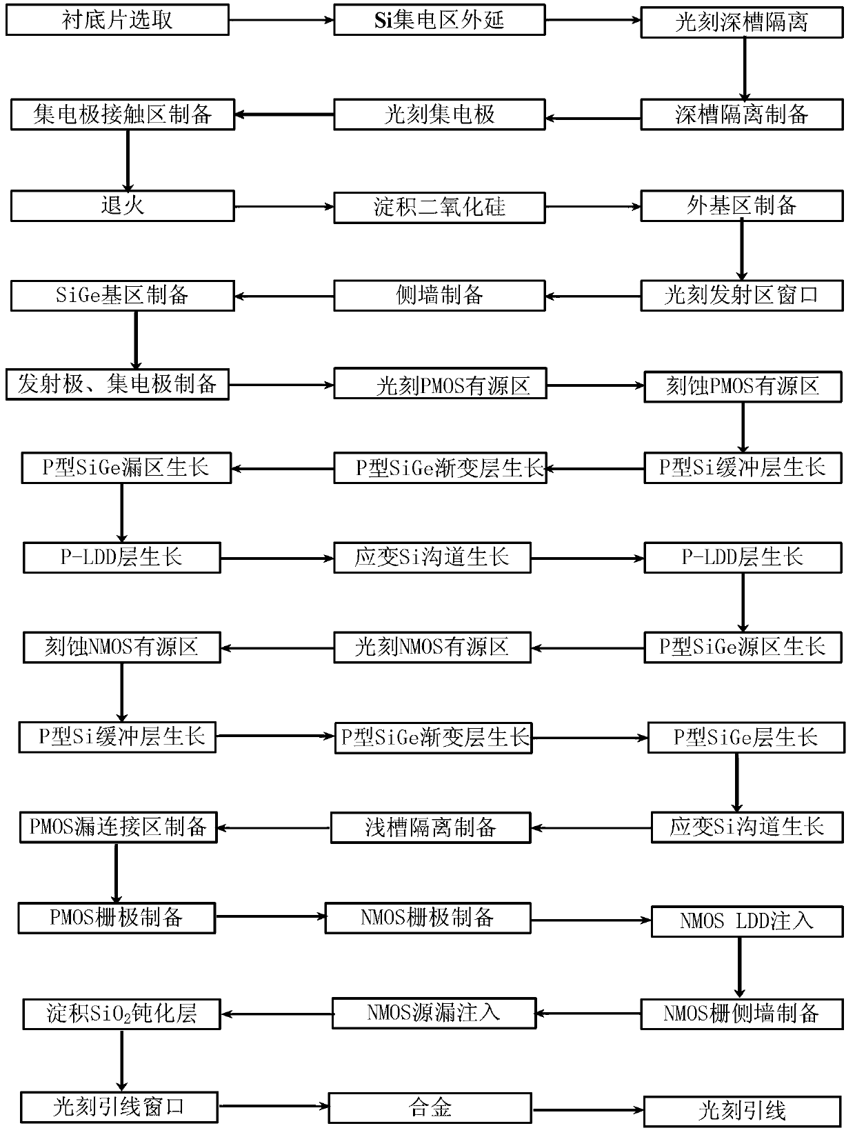
[0124] Embodiment 1: The preparation of strained Si, strained SiGe HBT BiCMOS integrated device and circuit with a channel length of 22nm, the specific steps are as follows:

[0125] Step 1, preparation of collector area and deep groove isolation.

[0126] (1a) Select the doping concentration to be 5×10 14 cm -3 A P-type Si sheet as a substrate;

[0127] (1b) Using chemical vapor deposition (CVD), at 600°C, deposit a SiO with a thickness of 300nm on the surface of the epitaxial Si layer. 2 Layer, photolithographic buried layer region, N-type impurities are implanted into the buried layer region to form N-type heavily doped buried layer region;

[0128] (1c) Etch the oxide layer on the surface of the substrate, and use chemical vapor deposition (CVD) to grow a layer of N-type epitaxial Si layer with a thickness of 1.5 μm on the upper Si material at 600 ° C, as a set electrical region, the doping concentration of this layer is 1×10 16 cm -3 ;

[0129] (1d) Deposit a layer...

Embodiment 2

[0197] Embodiment 2: The preparation of strained Si, strained SiGe HBT BiCMOS integrated devices and circuits with a channel length of 30nm, the specific steps are as follows:

[0198] Step 1, preparation of collector area and deep groove isolation.

[0199] (1a) Select the doping concentration as 1×10 15 cm -3 A P-type Si sheet as a substrate;

[0200] (1b) Using chemical vapor deposition (CVD), at 700 ° C, deposit a SiO with a thickness of 400 nm on the surface of the epitaxial Si layer. 2Layer, photolithographic buried layer region, N-type impurities are implanted into the buried layer region to form N-type heavily doped buried layer region;

[0201] (1c) Etch away the oxide layer on the surface of the substrate, and grow a layer of N-type epitaxial Si layer with a thickness of 1.8 μm on the upper Si material at 700 °C by chemical vapor deposition (CVD) as a set electrical region, the doping concentration of this layer is 5×10 16 cm -3 ;

[0202] (1d) Deposit a layer...

Embodiment 3

[0270] Embodiment 3: The strained Si, strained SiGe HBT BiCMOS integrated device and circuit that the channel length is prepared to be 45nm, concrete steps are as follows:

[0271] Step 1, preparation of collector area and deep groove isolation.

[0272] (1a) Select the doping concentration to be 5×10 15 cm -3 A P-type Si sheet as a substrate;

[0273] (1b) Using chemical vapor deposition (CVD), at 800 ° C, deposit a SiO with a thickness of 500 nm on the surface of the epitaxial Si layer. 2 Layer, photolithographic buried layer region, N-type impurities are implanted into the buried layer region to form N-type heavily doped buried layer region;

[0274] (1c) Etch away the oxide layer on the surface of the substrate, and grow an N-type epitaxial Si layer with a thickness of 2.5 μm on the upper Si material by chemical vapor deposition (CVD) at 800 °C, as a set electrical region, the doping concentration of this layer is 1×10 17 cm -3 ;

[0275] (1d) Deposit a layer of SiO...


PUM

PropertyMeasurementUnit
Thicknessaaaaaaaaaa
Thicknessaaaaaaaaaa
Thicknessaaaaaaaaaa

Abstract

The invention discloses a strained Si/strained SiGe-HBT BiCMOS integrated device and a preparation method. The preparation method comprises growing an N-type Si epitaxial layer on a substrate to serve as the collector region of the bipolar device, preparing deep trench isolation, and sequentially preparing base polysilicon, a base region, an emitter region and a collector to obtain the SiGe HBT device; preparing the active region of a PMOS (p-channel metal oxide semiconductor) device, and preparing a drain and a gate on the active region of the PMOS device to obtain the vertical-channel PMOS device; preparing the active region of an NMOS (n-channel metal oxide semiconductor) device, and preparing a gate dielectric layer and gate polysilicon on the active region of the NMOS device to obtain the NMOS device; and etching leads by lithography to obtain the strained Si/strained SiGe-HBT BiCMOS integrated device and circuit. According to the invention, the emitter, the base and the collector of the SiGe HBT all keep polysilicon contact, are prepared by self-alignment process and all have a full planar structure; and the prepared strained Si/strained SiGe-HBT BiCMOS integrated device is enhanced in performance by fully utilizing the characteristics of mobility anisotropy of the strained Si material in preparation of the MOS device.

Description

technical field [0001] The invention belongs to the technical field of semiconductor integrated circuits, and in particular relates to a strained Si / strained SiGe HBT device BiCMOS integrated device and a preparation method. Background technique [0002] Integrated circuits are the cornerstone and core of the economic development of an information society. Just as the American engineering and technology circle recently named the fifth electronic technology among the 20 greatest engineering and technological achievements in the world in the 20th century, "from vacuum tubes to semiconductors and integrated circuits, they have become the cornerstone of intelligent work in various industries today." Integrated circuits. It is one of the typical products that can best reflect the characteristics of knowledge economy. At present, the electronic information industry based on integrated circuits has become the world's largest industry. With the development of integrated circuit te...

Claims


Application Information

Patent Timeline
IPC IPC(8): H01L27/06H01L21/8249
Inventor 胡辉勇宣荣喜张鹤鸣宋建军王海栋舒斌李妤晨郝跃
Owner 西安电子科技大学重庆集成电路创新研究院
Why Eureka
Try Eureka