Preparation method of plated film member and plated film member prepared by method thereof
A technology for coating parts and prefabricated layers is applied in the field of the preparation of coating parts and the coating parts made therefrom, which can solve the problems such as limited color of the film layer, and achieve the effects of improving the competitiveness of appearance, avoiding abrasion and scratching, and maintaining stable performance.
- Summary
- Abstract
- Description
- Claims
- Application Information
AI Technical Summary
Problems solved by technology
Method used
Image
Examples
preparation example Construction
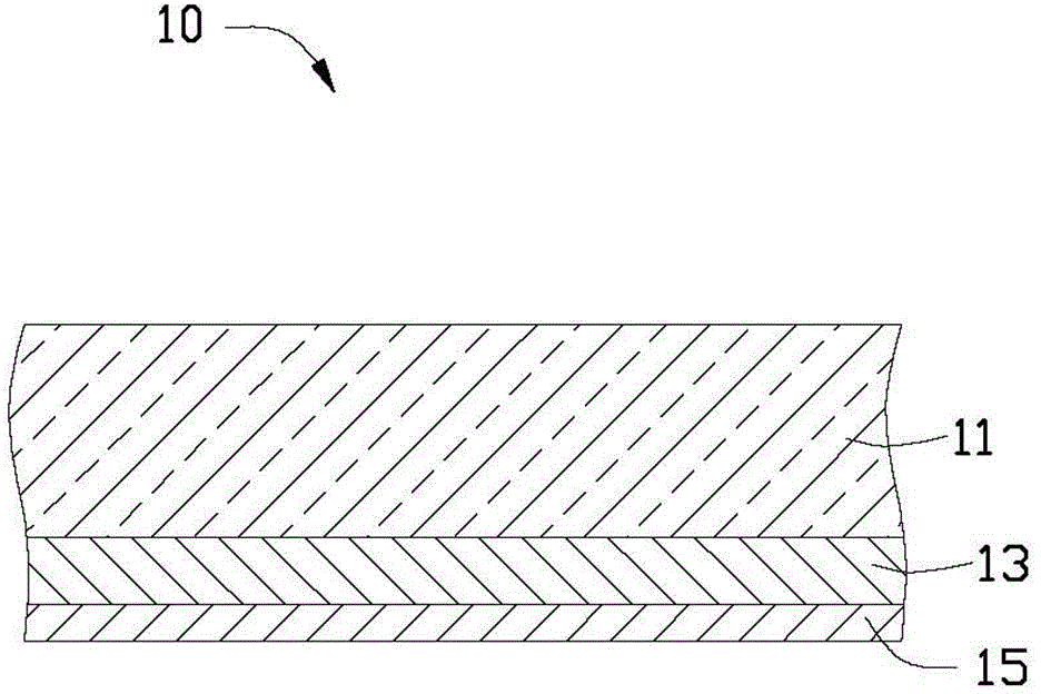
[0019] A coating member 10 of a preferred embodiment of the present invention (such as figure 1 Shown) the preparation method comprises the steps:
[0020] A substrate 11 is provided, and the substrate 11 is transparent glass.
[0021] The surface of the substrate 11 is pretreated. The pretreatment includes: conventional degreasing and wax removal, and then spraying the substrate 11 with deionized water, and drying the substrate 11 for future use after spraying.
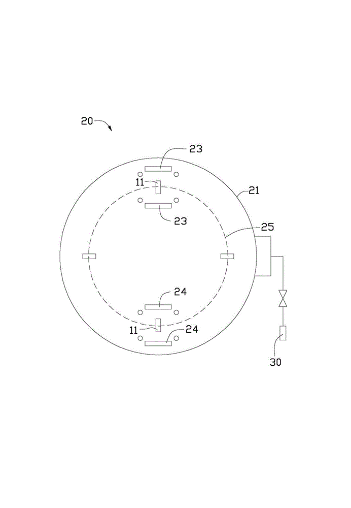
[0022] combined reference figure 2 , provide a vacuum coating machine 20, the vacuum coating machine 20 includes a coating chamber 21 and a vacuum pump 30 connected to the coating chamber 21, the vacuum pump 30 is used to evacuate the coating chamber 21. The coating chamber 21 is provided with a turntable (not shown), two aluminum targets 23 opposite to each other and two metal targets 24 opposite to each other. The turntable drives the base material 11 to revolve along the circular track 25 , and the base mater...
Embodiment 1
[0035] The vacuum coating machine 20 used in this embodiment is a magnetron sputtering coating machine.
[0036] Sputtering prefabricated layer A: the power of the aluminum target 23 is 13kW; the flow rate of the working gas argon is 300 sccm; the flow rate of the reaction gas oxygen is 100 sccm; the bias voltage applied to the substrate 11 is -50V, and the sputtering temperature is 100°C. The time is 20 minutes; the thickness of the prefabricated layer A is 120 nm.
[0037] Sputtering prefabricated layer B: the material of the metal target 24 used is aluminum, the power of the metal target 24 is 8kW; the flow rate of the working gas argon is 300 sccm; the bias voltage applied to the substrate 11 is -50V, and the sputtering time is 20min ; The thickness of the prefabricated layer B is 250nm.
[0038] Plasma bombardment: the bias voltage is -200V, and the bombardment time is 70min.
[0039] Repeat the above steps of sputtering prefabricated layer B and argon plasma bombardmen...
Embodiment 2
[0042] The vacuum coating machine 20 used in this embodiment is the same as that in Embodiment 1.
[0043] Sputtering prefabricated layer A: the power of the aluminum target 23 is 5kW; the flow rate of the working gas argon is 100 sccm; the flow rate of the reaction gas nitrogen is 500 sccm; the bias voltage applied to the substrate 11 is -10V, and the sputtering temperature is 180°C. The shooting time is 30min; the thickness of the prefabricated layer A is 80nm.
[0044] Sputtering prefabricated layer B: The material of the metal target 24 used is chromium, the power of the metal target 24 is 13kW; the flow rate of the working gas argon is 100 sccm; the bias voltage applied to the substrate 11 is -100V, and the sputtering time is 15min ; The thickness of the prefabricated layer B is 200nm.
[0045] Argon plasma bombardment: the bias voltage is -600V, and the bombardment time is 45min.
[0046]The above steps of sputtering prefabricated layer B and argon plasma bombardment w...
PUM
| Property | Measurement | Unit |
|---|---|---|
| thickness | aaaaa | aaaaa |
| thickness | aaaaa | aaaaa |
| thickness | aaaaa | aaaaa |
Abstract
Description
Claims
Application Information

