Method for preparing electromechanical transduction element based on potassium-sodium niobate lead-free piezoelectric nanofibers
A technology of potassium sodium niobate and nanofibers, applied in piezoelectric/electrostrictive/magnetostrictive devices, electrical components, nanotechnology for sensing, etc., can solve the constraints of poor repeatability and unfavorable nanogenerator construction , the limited length of nanorods, etc.
- Summary
- Abstract
- Description
- Claims
- Application Information
AI Technical Summary
Problems solved by technology
Method used
Image
Examples
Embodiment 1
[0096] Example 1: Preparation of an electromechanical transduction element based on potassium sodium niobate lead-free piezoelectric nanofibers
[0097] The steps of the preparation method are as follows:
[0098] Step A: Electrode Preparation
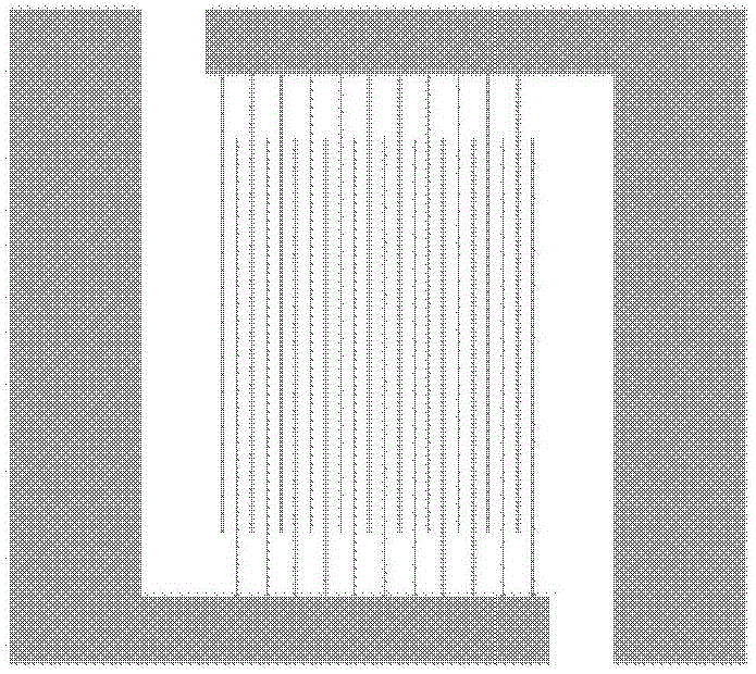
[0099] 1) Photolithography mask production: use the L-edit software sold by the American Tanner company to design the predetermined pattern of the interdigitated electrodes, and use the photolithography mask produced by Nanjing Qingwei Electronics Technology Co., Ltd., in which a single interdigitated electrode pattern The size is 1cm×1cm, the width of the interdigitated stripes is 10 μm and the spacing is 200 μm, and the number of interdigitated stripes is 20. The interdigitated electrode patterns are evenly and repeatedly arranged in a square with a side length of 70 mm to ensure that adjacent interdigitated electrodes The pattern spacing is not less than 2mm;
[0100] 2) Substrate cleaning: ultrasonically clean a P100 polished sil...
Embodiment 2
[0122] Example 2: Preparation of an electromechanical transduction element based on potassium sodium niobate lead-free piezoelectric nanofibers
[0123] The steps of the preparation method are as follows:
[0124] Step A: Electrode Preparation
[0125] 1) Photolithography mask production: use the L-edit software sold by American Tanner Company to design the predetermined pattern of interdigitated electrodes, and use Nanjing Qingwei Electronics Technology Co., Ltd. to order a photolithography mask, in which a single interdigitated electrode pattern The size is 1cm×1cm, the width of the interdigitated stripes is 20 μm and the spacing is 400 μm, and the number of interdigitated stripes is 50. The interdigitated electrode patterns are evenly and repeatedly arranged in a square with a side length of 70 mm to ensure that adjacent interdigitated electrodes The pattern spacing is not less than 2mm;
[0126] 2) Substrate cleaning: A P100 polished silicon oxide wafer with a diameter o...
Embodiment 3
[0148] Example 3: Preparation of an electromechanical transduction element based on potassium sodium niobate lead-free piezoelectric nanofibers
[0149] The steps of the preparation method are as follows:
[0150] Step A: Electrode Preparation
[0151] 1) Photolithography mask production: use the L-edit software sold by American Tanner Company to design the predetermined pattern of interdigitated electrodes, and use Nanjing Qingwei Electronics Technology Co., Ltd. to order a photolithography mask, in which a single interdigitated electrode pattern The size is 1cm×1cm, the width of the interdigitated stripes is 30 μm and the spacing is 600 μm, and the number of interdigitated stripes is 40. The interdigitated electrode patterns are evenly and repeatedly arranged in a square with a side length of 70 mm to ensure that adjacent interdigitated electrodes The pattern spacing is not less than 2mm;
[0152] 2) Substrate cleaning: A P100 polished silicon oxide wafer with a diameter o...
PUM
| Property | Measurement | Unit |
|---|---|---|
| diameter | aaaaa | aaaaa |
| thickness | aaaaa | aaaaa |
| diameter | aaaaa | aaaaa |
Abstract
Description
Claims
Application Information


