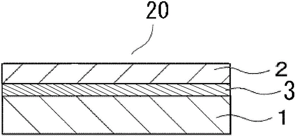
Adhesive tape for protecting surface of semiconductor wafer
A technology for semiconductors and wafers, applied in the field of tapes for surface protection of semiconductor wafers, can solve problems such as edge cracks and wafer breakage, and achieve the effects of reducing drop errors and warping
- Summary
- Abstract
- Description
- Claims
- Application Information
AI Technical Summary
Problems solved by technology
Method used
Image
Examples
Embodiment 1
[0136] With respect to 100 parts by weight of an acrylic copolymer having a weight-average molecular weight of 800,000 each having a radiation-curable carbon-carbon double bond-containing group, a hydroxyl group-containing group, and a carboxyl group-containing group, the mixed adduct-based isocyanate-based crosslinking agent Coronate 1 mass part of L (trade name, manufactured by Nippon Polyurethane Co., Ltd.) and 3 mass parts of photopolymerization initiator Irgacure 184 (trade name, manufactured by Ciba Japan Co., Ltd.) were adjusted with ethyl acetate to prepare an adhesive composition.
[0137] In addition, with respect to 100 parts by mass of an acrylic copolymer (acid value 10, hydroxyl value 2) containing n-butyl methacrylate as the main component and other components having hydroxyl and carboxyl groups, the adduct-based isocyanate 2 parts by mass of a crosslinking agent Coronate L (trade name, manufactured by Nippon Polyurethane Co., Ltd.) and 2 parts by mass of an epox...
Embodiment 2
[0149] With respect to 100 parts by mass of an acrylic copolymer having a weight average molecular weight of 800,000 each having a radiation-curable carbon-carbon double bond-containing group, a hydroxyl group-containing group, and a carboxyl group-containing group, the adduct-based isocyanate crosslinking agent Coronate L (trade name, manufactured by Nippon Polyurethane Co., Ltd.) and 3 parts by mass of photopolymerization initiator Irgacure 184 (trade name, manufactured by Ciba Japan Co., Ltd.) were adjusted with ethyl acetate to prepare an adhesive composition.
[0150] In addition, with respect to 100 parts by mass of an acrylic copolymer (acid value 11, hydroxyl value 3) having n-butyl methacrylate as the main component and other components having hydroxyl and carboxyl groups, the adduct-based isocyanate 1 part by mass of the crosslinking agent Coronate L (trade name, manufactured by Nippon Polyurethane Co., Ltd.) and 2 parts by mass of the epoxy-based crosslinking agent T...
Embodiment 3
[0154] With respect to 100 parts by mass of an acrylic copolymer having a weight average molecular weight of 800,000 each having a radiation-curable carbon-carbon double bond-containing group, a hydroxyl group-containing group, and a carboxyl group-containing group, the adduct-based isocyanate crosslinking agent Coronate L (trade name, manufactured by Nippon Polyurethane Co., Ltd.) and 3 parts by mass of photopolymerization initiator Irgacure 184 (trade name, manufactured by Ciba Japan Co., Ltd.) were adjusted with ethyl acetate to prepare an adhesive composition.
[0155] In addition, an isocyanate crosslinking agent TKA-100 (trade name, manufactured by Asahi Kasei Chemical Co., Ltd.) was mixed with respect to 100 parts by mass of an acrylic copolymer (hydroxyl value: 35) having n-butyl methacrylate as one of its constituents and having a hydroxyl group. 12 parts by mass, the concentration was adjusted with ethyl acetate to prepare an intermediate resin layer composition.
[...
PUM
| Property | Measurement | Unit |
|---|---|---|
| length | aaaaa | aaaaa |
| glass transition temperature | aaaaa | aaaaa |
| thickness | aaaaa | aaaaa |
Abstract
Description
Claims
Application Information
 - R&D
- Intellectual Property
- Life Sciences
- Materials
- Tech Scout
- Unparalleled Data Quality
- Higher Quality Content
- 60% Fewer Hallucinations
Browse by: Latest US Patents, China's latest patents, Technical Efficacy Thesaurus, Application Domain, Technology Topic, Popular Technical Reports.
© 2025 PatSnap. All rights reserved.Legal|Privacy policy|Modern Slavery Act Transparency Statement|Sitemap|About US| Contact US: help@patsnap.com

