Method for forming holes in substrate of nitride device by mixing type etching

A nitride and hybrid technology, applied in semiconductor devices, semiconductor/solid-state device manufacturing, electrical components, etc., can solve problems such as poor selectivity and difficult laser operation, and achieve the effect of improving yield and ensuring efficiency

Inactive Publication Date: 2012-11-07
JIANGSU YANGJING OPTOELECTRONICS
View PDF5 Cites 1 Cited by
  • Summary
  • Abstract
  • Description
  • Claims
  • Application Information

AI Technical Summary

Problems solved by technology

[0010] The biggest problem of laser opening is the poor selectivity. For the opening of nitride microwave and power devices and integrated circuits, it is hoped that the opening surface stays on the metal layer on the front side of the substrate. For the opening of nitride optoelectronic devices and integrated circuits, it is hoped that the opening surface stays The epitaxial semiconductor layer on the front side of the substrate, the operation accuracy of the typical process is about 1-3 microns, which is very difficult for the operation of the laser
Assuming that the target penetration depth is 100 μm, considering the unevenness of the substrate surface and the fluctuation of laser power, the use of high-energy laser alone is not suitable for the opening process of sapphire substrates and silicon carbide (SiC) substrates.

Method used


Image

  • Method for forming holes in substrate of nitride device by mixing type etching
  • Method for forming holes in substrate of nitride device by mixing type etching
  • Method for forming holes in substrate of nitride device by mixing type etching

Examples


Embodiment 1

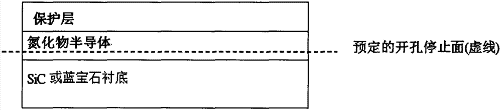
[0031] Example 1: Hole stopped in nitride semiconductor on substrate

[0032] Such as Figure 1 to Figure 4 As shown, the process is as follows:

[0033] (1) if figure 1 As shown, the other side of the opening is protected.

[0034] On the backside of the processed surface of the semiconductor wafer, a water-soluble resist was evenly applied to the entire surface with a spin coater, and dried to form a protective film with a thickness of 2 μm.

[0035]When a laser processing machine is irradiated, the dirt scatters violently and adheres to the front and back of the semiconductor wafer during processing. As a result of EDX (Energy Dispersive X-ray, X-ray energy spectrum quantitative analysis) analysis of the dirt with an electron microscope (FE-SEM), it is Al, O, C, Cl, Si with the composition of compound semiconductors and substrates Equivalent to at least one elemental composition. Therefore, the reverse side of the processed surface is covered with a protective layer be...

Embodiment 2

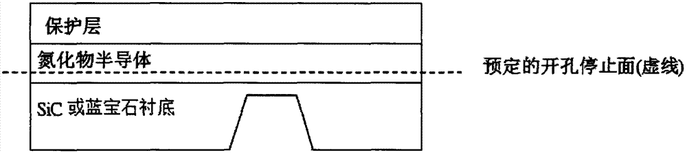
[0050] Embodiment 2: as Figure 5 As shown, the difference between this embodiment and Embodiment 1 lies in that: the opening stops at the metal layer on the substrate.

Embodiment 3

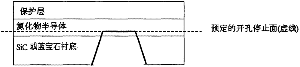
[0051] Embodiment 3: as Figure 6 As shown, the difference between this embodiment and Embodiment 1 lies in that the opening penetrates the nitride semiconductor on the surface of the substrate and stops on the metal layer on the nitride semiconductor.


PUM

PropertyMeasurementUnit
angleaaaaaaaaaa
thicknessaaaaaaaaaa
thicknessaaaaaaaaaa

Abstract

The invention discloses a method for forming holes in a substrate of a nitride device by mixing type etching. The method comprises the following steps of: perforating a large part of the substrate of the nitride device by using laser, wherein the target depth of the hole is not more than 10 microns; and perforating the rest part of the substrate of the nitride device by dry etching, wherein the depth of the rest part is not more than 10 microns. By the method, the perforating speed is high, and the precision is high.

Description

technical field [0001] The invention relates to a manufacturing process of a nitride device and an integrated circuit, in particular to a method for hybrid etching to produce a hole in a nitride device substrate. Background technique [0002] Nitride is one of compound semiconductors, and nitride semiconductors are often used in optoelectronics, microwave and power fields. Nitride semiconductors are often used in the field of optoelectronics, because gallium nitride (GaN) has an energy gap of 3.4eV, so it can be made into optoelectronic devices such as blue / green light, ultraviolet light-emitting diodes, lasers, and photodetectors. Nitride semiconductors are often used in microwave and high-power fields, because nitride semiconductors have high energy gap characteristics, so they can be used in microwave devices, power devices, microwave integrated circuits, power integrated circuits, such as field effect transistors, power amplifiers. [0003] The growth method of the semi...

Claims


Application Information

Patent Timeline
Patent Type & Authority Applications(China)
IPC IPC(8): H01L21/302
CPCH01L21/3065H01L29/1608
Inventor 廖丰标顾玲
Owner JIANGSU YANGJING OPTOELECTRONICS
Why Eureka
Try Eureka