
Semiconductor device with trench super junction MOS (metal oxide semiconductor) structure and manufacturing method thereof

A MOS structure and semiconductor technology, applied in semiconductor/solid-state device manufacturing, semiconductor devices, electrical components, etc., can solve problems such as increasing channel length, increasing on-resistance and on-voltage drop, increasing impurity doping concentration, etc. , to achieve the effect of low on-resistance, easy inversion, and low turn-on voltage drop

Inactive Publication Date: 2012-11-07
朱江
View PDF0 Cites 1 Cited by
  • Summary
  • Abstract
  • Description
  • Claims
  • Application Information

AI Technical Summary

Problems solved by technology

When increasing the reverse breakdown voltage between the body region 3 source region 4 and the drain region 2 of the device, it is necessary to increase the channel length or increase the impurity doping concentration in the region where the channel is located, and at the same time reduce the doping of the drain region 2 concentration or increase the thickness of the drain region 2, thus causing an increase in the on-resistance and on-voltage drop between the source region 4 and the drain region 2 of the device
[0004] The traditional manufacturing method of super junction structure is realized by repeated injection annealing and epitaxial layer growth on the semiconductor material, which greatly improves the production cost of the device, the production cycle and the difficulty of process control.

Method used


Image

  • Semiconductor device with trench super junction MOS (metal oxide semiconductor) structure and manufacturing method thereof
  • Semiconductor device with trench super junction MOS (metal oxide semiconductor) structure and manufacturing method thereof
  • Semiconductor device with trench super junction MOS (metal oxide semiconductor) structure and manufacturing method thereof

Examples


Embodiment Construction

[0030] first embodiment

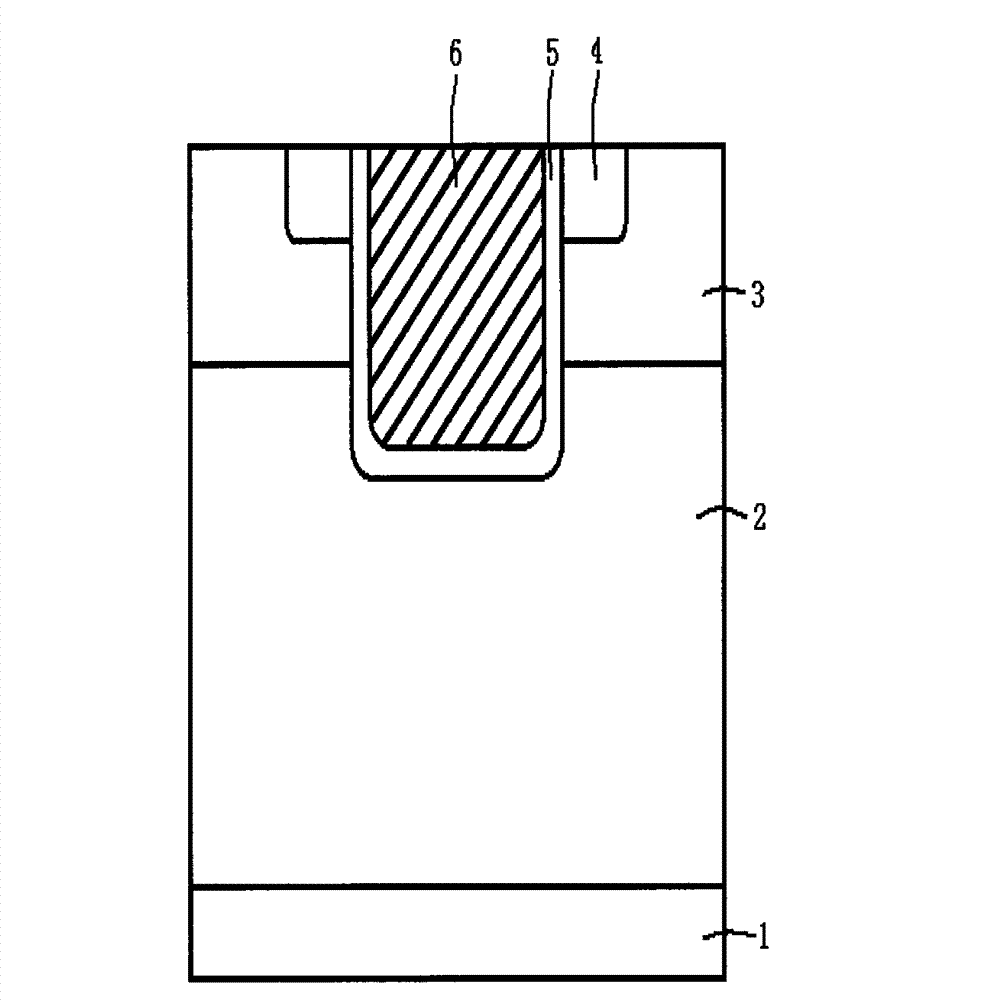
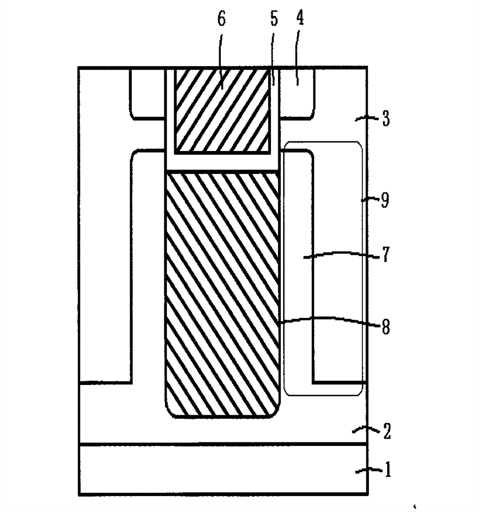
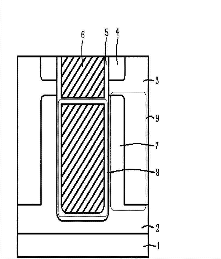
[0031] figure 2 It is a schematic cross-sectional view of a trench superjunction MOS structure semiconductor device of the present invention, combined below figure 2 The semiconductor device of the present invention and its manufacturing method will be described in detail.

[0032] A semiconductor device with a trench superjunction MOS structure, comprising: a substrate layer 1, which is an N conductivity type silicon semiconductor material; a drain region 2, located on the substrate layer 1, which is an N conductivity type silicon semiconductor material; a body region 3, which is located at Above the drain region 2, the body region 3 is a silicon semiconductor material of P conductivity type; the source region 4 is located in the upper surface of the body region 3 and is a silicon semiconductor material of N conductivity type; the super junction drain region 7 is a trench and a body The silicon semiconductor material of N conductivity type betwee...


PUM


Abstract

The invention relates to a semiconductor device with a trench super junction MOS (metal oxide semiconductor) structure, and further relates to a manufacturing method of the semiconductor device with the trench super junction MOS structure. The manufacturing method comprises the step of arranging a super junction structure into semiconductor materials between trenches, so that the manufacturing process of the super junction structure is simplified; and the device is a basic structure for manufacturing a power MOSFET (metal-oxide-semiconductor field effect transistor) device and a super potential barrier rectifier.

Description

technical field [0001] The invention relates to a semiconductor device with a trench superjunction MOS structure, which is the basic structure of a super barrier rectifier and a power MOSFET device. The invention also relates to a preparation method for a semiconductor device with a trench superjunction MOS structure. Background technique [0002] Semiconductor devices with trench structures and super junction structures have become an important trend in device development. For power semiconductor devices, the requirement to continuously reduce the on-resistance and continuously increase the current density has become an important trend in the development of devices. [0003] The cross-sectional view of a conventional trench MOS device is shown in figure 1 As shown, gate oxide 5 is grown on the entire inner wall of the vertical trench, gate polysilicon 6 is filled in the trench, and active region 4 , body region 3 and drain region 2 are arranged from top to bottom in the si...

Claims


Application Information

Patent Timeline
Patent Type & Authority Applications(China)
IPC IPC(8): H01L29/78H01L29/06H01L29/10H01L21/336H01L21/28
Inventor 朱江
Owner 朱江
Learn More