Insulated gate bipolar transistor (IGBT) with deep energy level impurity implantation

A technology of bipolar transistors and deep-level impurities, which is applied to semiconductor devices, electrical components, circuits, etc., can solve the problems of device avalanche breakdown, small conduction voltage drop, and increased leakage current, and achieve accelerated recombination, reduced Small high temperature leakage current, the effect of reducing the overall power consumption

Inactive Publication Date: 2012-11-14
UNIV OF ELECTRONIC SCI & TECH OF CHINA +1
View PDF3 Cites 10 Cited by
  • Summary
  • Abstract
  • Description
  • Claims
  • Application Information

AI Technical Summary

Problems solved by technology

[0003] When the IGBT is forward-conducting, the positive gate voltage makes the channel open, and the emitter electrons flow through the channel to the drift region. Due to the forward bias of the collector, a large number of holes in the collector region flood into the drift region, and the drift region A large number of electrons have a conductance modulation effect, which can make the turn-on voltage drop of the IGBT much smaller than that of the VDMOS; when the IGBT is turned off, the gate voltage is negative voltag

Method used


Image

  • Insulated gate bipolar transistor (IGBT) with deep energy level impurity implantation
  • Insulated gate bipolar transistor (IGBT) with deep energy level impurity implantation
  • Insulated gate bipolar transistor (IGBT) with deep energy level impurity implantation

Examples


Example Embodiment

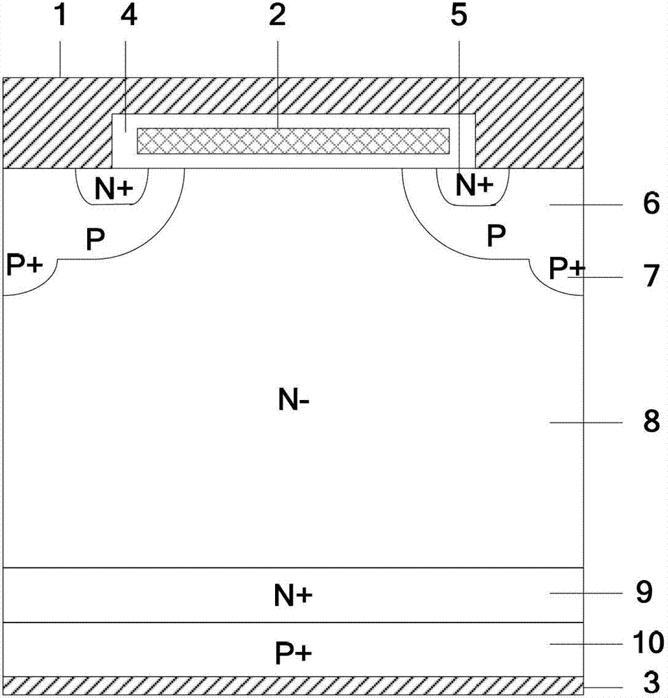
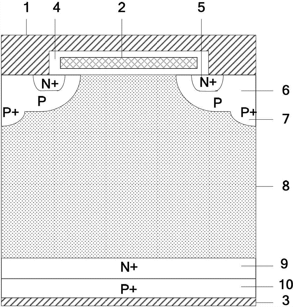
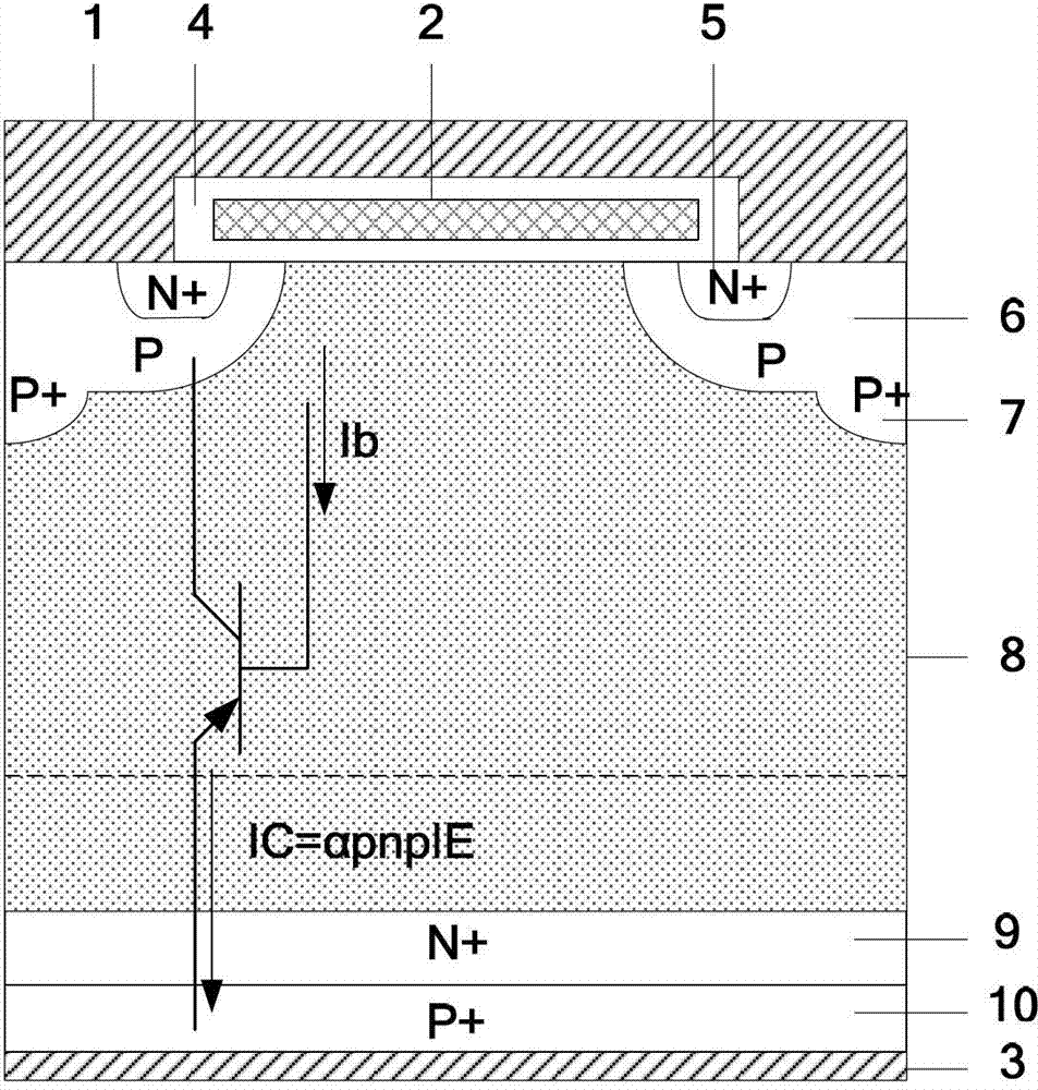
[0018] An insulated gate bipolar transistor with deep-level impurity implantation. Its cell structure is as figure 2 As shown, it includes an active emitter 1, a polysilicon gate electrode 2, a metal collector 3, a silicon dioxide gate oxide layer 4, an N+ active region 5, a P-type base region 6, a P+ body region 7, and an N- drift region 8. , N+ electric field stop layer 9, P+ collector region 10; from the bottom layer to the top, the device is metalized collector 3, P+ collector region 10, N+ electric field stop layer 9, N- drift region 8, and P-type base region 6 is located On both sides of the top of the N- drift region 8, the P-type base region 6 has an N+ active region 5, and the P+ body region 7 is located on both sides of the N- drift region 8 below the P-type base region 6, and is connected to the P-type base region 6 and The N- drift region 8 is in contact with each other; the active emitter 1 is in contact with the N+ active region 5 and the P-type base region 6 on b...


PUM


Abstract

The invention discloses an insulated gate bipolar transistor (IGBT) with deep energy level impurity implantation and belongs to the technical field of semiconductor power devices. Deep energy level N-type impurities are implanted into an N-drift region (8) on the basis of the traditional Planar FS-IGBT. According to the characteristic that the ionization degree of the deep energy level impurities is raised and the impurity concentration is raised along with the temperature increase, the parasitic PNP transistor alpha PNP of the IGBT can be effectively reduced, so that the high-temperature leakage current of the IGBT is reduced, and the overall loss of the IGBT is reduced further; and moreover, the electron concentration increased in the N-drift region (8) and holes in the drift region are accelerated and compounded, and the deep energy level impurity self is a deathnium, the electron hole recombination is accelerated, the turnoff process of the IGBT is reduced, the turnoff characteristics are effectively improved, and the reliability of the IGBT is improved.

Description

technical field [0001] The invention belongs to the technical field of semiconductor power, and relates to an insulated gate bipolar transistor (Insulate Gate Bipolar Transistor, IGBT for short). Background technique [0002] Insulated-gate bipolar transistor (IGBT), as a representative of power electronic devices, is the product of choice for improving performance and energy-saving indicators of the whole machine. IGBT not only has the advantages of high input impedance, low control power, simple driving circuit and high switching speed of MOSFET, but also has the advantages of high current density, low saturation voltage and strong current handling ability of bipolar power transistor. Therefore, the three major characteristics of IGBT power devices are high voltage, high current, and high speed, which are unmatched by other power devices. Therefore, it is an ideal switching device in the field of power electronics. IGBT products combine three technical advantages of high ...

Claims


Application Information

Patent Timeline
IPC IPC(8): H01L29/36H01L29/739
Inventor 李泽宏李巍张蒙李长安张金平任敏张波
Owner UNIV OF ELECTRONIC SCI & TECH OF CHINA
Why Eureka
Try Eureka