A multi-layer composite film passivation structure and preparation process for mesa high-power semiconductor devices

A multi-layer composite film and semiconductor technology, applied in the fields of semiconductor/solid-state device manufacturing, semiconductor devices, semiconductor/solid-state device components, etc., can solve the problems of inconsistent thermal expansion coefficient, device surface composite enhancement, high surface state density, etc. The effect of reducing lattice defects, repairing lattice damage, alleviating lattice stress and thermal stress

Active Publication Date: 2016-06-15
江苏吉莱微电子股份有限公司
View PDF6 Cites 0 Cited by
  • Summary
  • Abstract
  • Description
  • Claims
  • Application Information

AI Technical Summary

Problems solved by technology

However, the single-layer glass passivation process has inconsistent thermal expansion coefficients between glass and silicon wafers, which easily leads to chip breakage under thermal stress, and glass is an insulating medium, which cannot shield the external electric field and cannot modulate the surface electric field of the pn junction on the table. Boron-containing glass The semiconductor will also be doped to make the device low breakdown, so the passivation effect is limited, and the reliability of single-layer glass passivated high-voltage devices working under high temperature and high pressure conditions is also low
[0003] The role of the α-polysilicon layer is: the mesa power semiconductor device usually adopts the wet etching method of hydrofluoric acid + concentrated nitric acid + glacial acetic acid during the mesa molding process. After the groove is etched, the groove is relatively rough. More importantly, the corrosion will As a result, lattice defects and higher surface state density will be generated in the groove, the device surface recombination will be greatly enhanced, and the leakage current will be larger

Method used


Image

  • A multi-layer composite film passivation structure and preparation process for mesa high-power semiconductor devices
  • A multi-layer composite film passivation structure and preparation process for mesa high-power semiconductor devices

Examples


Embodiment 1

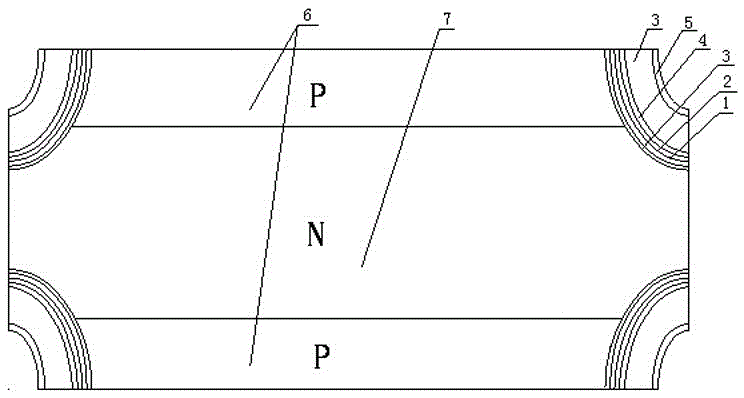
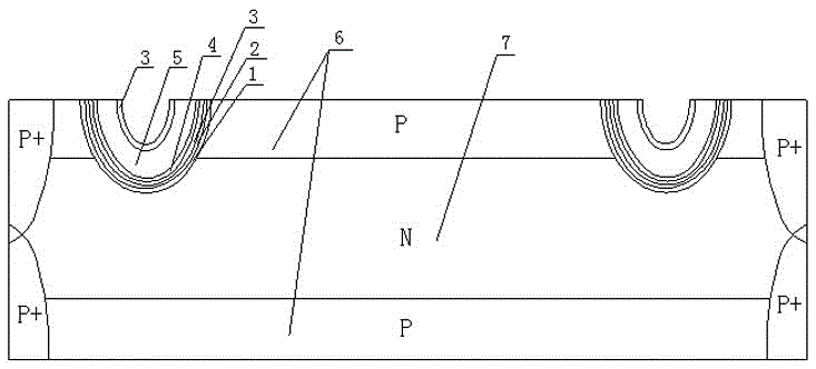
[0024] A preparation process for a multilayer composite film passivation structure of a mesa high-power semiconductor device includes the following process steps in sequence:

[0025] a. Deposit α-polysilicon by LPCVD at a temperature of 570°C and a pressure of 0.3Torr, SiH 4 Flow rate 40cc / min, deposition time 4min;

[0026] b. Deposit semi-insulating polysilicon, using LPCVD deposition, the temperature is 650°C, the pressure is 0.3Torr, SiH 4 Flow 250cc / min, N 2 O flow rate 40cc / min, deposition time 40min;

[0027] c. Deposit a low-temperature thermal oxide layer, using LPCVD deposition, the temperature is 420 ° C, the pressure is 0.3 Torr, SiH 4 Flow 150cc / min, O 2 Flow rate 40cc / min, deposition time 20min;

[0028] d. Deposit Si 3 N 4 , using LPCVD deposition, the temperature is 750 ℃, the pressure is 0.3Torr, SiH 2 Cl 2 Flow 150cc / min, NH 3 Flow rate 400cc / min, deposition time 20min;

[0029] e. Glass passivation, apply lead aluminosilicate glass by scraping me...

Embodiment 2

[0032] A preparation process for a multilayer composite film passivation structure of a mesa high-power semiconductor device includes the following process steps in sequence:

[0033] a. Deposit α-polysilicon, using LPCVD deposition, the temperature is 575°C, the pressure is 0.35Torr, SiH 4 Flow rate 40cc / min, deposition time 4.5min;

[0034] b. Deposit semi-insulating polysilicon, using LPCVD deposition, the temperature is 660°C, the pressure is 0.3Torr, SiH 4 Flow 250cc / min, N 2O flow rate 40cc / min, deposition time 45min;

[0035] c. Deposit a low-temperature thermal oxide layer, using LPCVD deposition, the temperature is 435 ° C, the pressure is 0.3 Torr, SiH 4 Flow 150cc / min, O 2 Flow rate 40cc / min, deposition time 25min;

[0036] d. Deposit Si 3 N 4 , using LPCVD deposition, the temperature is 770 ℃, the pressure is 0.4Torr, SiH 2 Cl 2 Flow 150cc / min, NH 3 Flow rate 400cc / min, deposition time 25min;

[0037] e. Glass passivation, use the method of scraping to c...

Embodiment 3

[0040] A preparation process for a multilayer composite film passivation structure of a mesa high-power semiconductor device includes the following process steps in sequence:

[0041] a. Deposit α-polycrystalline silicon by LPCVD at a temperature of 580°C and a pressure of 0.4Torr, SiH 4 Flow rate 40cc / min, deposition time 5min;

[0042] b. Deposit semi-insulating polysilicon, using LPCVD deposition, the temperature is 670°C, the pressure is 0.3Torr, SiH 4 Flow 250cc / min, N 2 O flow rate 40cc / min, deposition time 50min;

[0043] c. Deposit a low-temperature thermal oxide layer by LPCVD at a temperature of 450°C and a pressure of 0.3Torr, SiH 4 Flow 150cc / min, O 2 Flow rate 40cc / min, deposition time 30min;

[0044] d. Deposit Si 3 N 4 , using LPCVD deposition, the temperature is 800 ℃, the pressure is 0.5Torr, SiH 2 Cl 2 Flow 150cc / min, NH 3 Flow rate 400cc / min, deposition time 30min;

[0045] e. Glass passivation, use the method of scraping to coat lead aluminosilic...


PUM


Abstract

The invention discloses a multilayer composite membrane passivation structure of a table top high-power semiconductor device. The multilayer composite membrane passivation structure comprises P-type boron junction areas and an N-type phosphorus junction area, the upper end and the lower end of the N-type phosphorus junction area are provided with the P-type phosphorus areas respectively, and an alpha-polycrystalline silicon layer, a semi-insulating polycrystalline silicon thin membrane, a low-temperature heat oxidation layer, a high-temperature Si3N4 thin membrane, a negative charge glass passivation layer and a low-temperature heat oxidation layer are sequentially arranged on the surface of a PN junction of a table top of the table top high-power semiconductor device from inside to outside. A manufacturing technology of the multilayer composite membrane passivation structure of the table top high-power semiconductor device includes the following steps: a, depositing the alpha-polycrystalline silicon, b, depositing semi-insulating polycrystalline silicon, c, depositing the low-temperature heat oxidation layer, d, depositing Si3N4, e, conducting passivation on glass, and f, depositing the low-temperature heat oxidation layer in the outmost layer. The multilayer composite membrane passivation structure and the manufacturing technology have the advantages that the alpha-polycrystalline silicon layer is deposited, so that crystal lattice adaptation can be achieved, damage to crystal lattices of a silicon wafer in a groove can be repaired, leaked currents in the surfaces of junctions are reduced, and the stability and the reliability of the device at the high temperature are improved.

Description

technical field [0001] The invention relates to a multilayer composite film passivation structure of a mesa high-power semiconductor device, and also relates to a preparation process of the multilayer composite film passivation structure of a mesa high-power semiconductor device. Background technique [0002] In order to prevent surface contamination, it is usually necessary to cover the surface of the semiconductor device with a protective dielectric film to form a passivation layer. The passivation process of high-voltage and high-power semiconductor devices on the mesa generally adopts single-layer glass passivation. Glass passivation can effectively prevent the pn junction contamination on the mesa, and as a terminal structure, improve the surface breakdown characteristics of high-voltage devices on the mesa, so that high-voltage semiconductor devices can obtain Voltage blocking capability. However, the single-layer glass passivation process has inconsistent thermal exp...

Claims


Application Information

Patent Timeline
Patent Type & Authority Patents(China)
IPC IPC(8): H01L23/31H01L23/29H01L21/56C30B28/14C23C16/34C23C16/40
CPCH01L23/3178H01L23/3171H01L2924/0002
Inventor 刘宗贺邹有彪张鹏王泗禹耿开远周健李建新
Owner 江苏吉莱微电子股份有限公司
Why Eureka
Try Eureka