Composite passivation film for semiconductor device and preparation method thereof

A passivation film, semiconductor technology, applied in the direction of semiconductor devices, semiconductor/solid-state device manufacturing, semiconductor/solid-state device components, etc., can solve the problems of inconsistent thermal expansion coefficient, device surface composite enhancement, high surface state density, etc., to reduce Lattice defects, passivation of surface charges, and the effect of increasing operating junction temperature

Active Publication Date: 2019-05-10
富芯微电子有限公司
View PDF4 Cites 0 Cited by
  • Summary
  • Abstract
  • Description
  • Claims
  • Application Information

AI Technical Summary

Problems solved by technology

However, the single-layer glass passivation process has inconsistent thermal expansion coefficients between glass and silicon wafers, which easily leads to chip breakage under thermal stress, and glass is an insulating medium, which cannot shield the external electric field and cannot modulate the surface electric field of the pn junction on the table. Boron-containing glass The semiconductor will also be doped to make the device low breakdown, so the passivation effect is limited, and the reliability of single-layer glass passivated high-voltage devices working under high temperature and high pressure conditions is also low
[0003] Mesa power semiconductor devices usually adopt the wet etching method of hydrofluoric acid + concentrated nitric acid + glacial acetic acid in the process of mesa molding. After the groove is etched, the groove is relatively rough. More importantly, the corrosion will cause lattice defects and Higher surface state density, the surface recombination of the device will be greatly enhanced, and the leakage current will be larger

Method used


Image

  • Composite passivation film for semiconductor device and preparation method thereof
  • Composite passivation film for semiconductor device and preparation method thereof

Examples


Embodiment 1

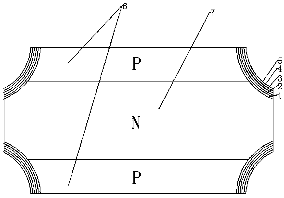
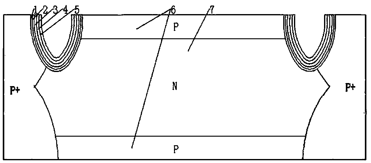
[0031] Such as figure 1 or figure 2 Shown, a kind of compound passivation film of semiconductor device of the present invention, described passivation film comprises five-layer structure, one layer is positioned at the polysilicon film layer 1 on the base, is arranged on the SIPOS film layer 2 on the polysilicon layer 1, sets The LTO film layer 3 on the SIPOS film layer 2 also includes a PSG film layer 4 disposed on the LTO film layer 3 , and an oxygen-enriched silicon dioxide film layer 5 on the PSG film layer 4 .

[0032] The above is the core of the present invention, the polysilicon layer 1 of the composite film passivation film of the semiconductor device can realize lattice adaptation, repair the damage of the silicon chip lattice in the groove, and reduce the junction surface leakage current; the SIPOS film layer 2, the shielding can The influence of moving ions and external electric field on the device can improve the breakdown voltage of the device and reduce the hi...

Embodiment 2

[0039] A process for preparing a composite passivation film for a semiconductor device. The passivation film includes a five-layer film formed by low-pressure chemical vapor deposition. The temperature of the PSG film layer is 420 °C and the pressure is 0.2 °C. Torr; the temperature for low-pressure chemical vapor deposition of the oxygen-increased silicon dioxide layer is 420°C and the pressure is 0.3t, and the temperature for high-temperature densification is 780°C and the pressure is 0.01Torr.

[0040] Specifically, the passivation film includes the following process steps:

[0041] Step 1: Deposit polysilicon by using low-pressure chemical vapor deposition at a temperature of 560°C and a pressure of 0.2Torr, SiH 4 Flow rate 50cc / min, deposition time 6min;

[0042] Step 2, deposit SIPOS at a temperature of 650°C and a pressure of 0.3Torr, SiH 4 The flow rate is 250cc / min, the N2O flow rate is 40cc / min, and the deposition time is 55min;

[0043] Step 3, depositing the LTO...

Embodiment 3

[0049] A process for preparing a composite passivation film for a semiconductor device. The passivation film includes a five-layer film formed by low-pressure chemical vapor deposition. The temperature of the PSG film layer is 450°C and the pressure is 0.4 Torr; the temperature for low-pressure chemical vapor deposition of the oxygen-enriched silicon dioxide layer is 445° C. and the pressure is 0.3 Torr, and the temperature for high-temperature densification is 820° C. and the pressure is 0.03 Torr.

[0050] Specifically, the passivation film includes the following process steps:

[0051] Step 1: Deposit polysilicon by using low-pressure chemical vapor deposition at a temperature of 580°C and a pressure of 0.4Torr, SiH 4 Flow rate 50cc / min, deposition time 10min;

[0052] Step 2, deposit SIPOS at a temperature of 670°C and a pressure of 0.3Torr, SiH 4 The flow rate is 250cc / min, the N2O flow rate is 40cc / min, and the deposition time is 60min;

[0053] Step 3, deposit the LT...


PUM


Abstract

The invention belongs to the semiconductor production technology field and especially relates to a semiconductor-device composite passive film. The passive film comprises five layer structures. The structures are characterized in that one layer is a polysilicon film layer located on a substrate; a SIPOS film layer is arranged on a polysilicon layer; a LTO film layer is arranged on the SIPOS film layer; a PSG film layer is arranged on the LTO film layer; and an oxygenation silicon dioxide film layer is located on the PSG film layer. In the invention, through using a low pressure chemical meteorological deposition mode, the five layers of films are successively deposited so that the composite films are interacted and form a system; junction surface passivation performance of a table-board large-power semiconductor device is effectively improved; the film can bear above 1600V voltage; a leakage current of a device is reduced; high temperature work stability and reliability of the device are increased; a work junction temperature of the device is increased; and a product yield rate of a production line is greatly increased.

Description

technical field [0001] The invention belongs to the technical field of semiconductor production, in particular to a composite passivation film for semiconductor devices and a preparation method thereof. Background technique [0002] The passivation process of semiconductor devices generally adopts single-layer glass passivation. Glass passivation can effectively prevent the contamination of the mesa pn junction, and can improve the surface breakdown characteristics of the mesa high-voltage devices, so that the high-voltage semiconductor devices can obtain stable voltage blocking capabilities. However, the single-layer glass passivation process has inconsistent thermal expansion coefficients between glass and silicon wafers, which easily leads to chip fragmentation under thermal stress, and glass is an insulating medium, which cannot shield the external electric field and cannot modulate the electric field on the pn junction surface of the table. Boron-containing glass The se...

Claims


Application Information

Patent Timeline
Patent Type & Authority Patents(China)
IPC IPC(8): H01L23/29H01L21/02
CPCH01L2924/10155
Inventor 刘宗贺纪锦程邹有彪李超
Owner 富芯微电子有限公司
Why Eureka
Try Eureka