A kind of aluminum oxide thin film and preparation method and application thereof
A kind of aluminum oxide and thin film technology, which is applied in the direction of solid state chemical plating, metal material coating technology, transistors, etc., can solve the problems affecting the performance of thin film, and achieve the effect of increased moldability, excellent insulation performance and uniform thin film structure
- Summary
- Abstract
- Description
- Claims
- Application Information
AI Technical Summary
Problems solved by technology
Method used
Image
Examples
Embodiment 1
[0054] The preparation method of aluminum oxide thin film, comprises the following steps:
[0055] (1) Preparation of aluminum precursor solution
[0056] According to the thickness of alumina to be prepared, take a certain amount of aluminum precursor material - aluminum nitrate and stabilizer - monoethanolamine dissolved in propylene glycol monomethyl ether, stir well until the solution is clear, the stirring process is about 4 hours , to obtain a precursor solution, which is left to stand for use, wherein the molar ratio of aluminum nitrate and monoethanolamine added is: 1:3.
[0057] (2) Preparation of alumina semiconductor thin film
[0058] The reaction solution prepared in step (1) is coated on the coating surface by spin coating to form a film. The coating surface of the present invention can be a substrate or a semiconductor layer according to the structure of the transistor device. The coating in this embodiment The surface is a glass substrate. Under the air atmo...
Embodiment 1-1
[0072] The preparation method of aluminum oxide thin film, comprises the following steps:
[0073] (1) Preparation of aluminum precursor solution
[0074] Same as Example 1
[0075] (2) Preparation of alumina semiconductor thin film
[0076] The heat treatment program is to start heating at 200°C, raise the temperature at a rate of 60°C / min, and raise the temperature to a predetermined temperature of 400°C, continue heat treatment for at least 30 minutes, and cool naturally to room temperature. The remaining steps are the same as implementation 1.
[0077] A thin film transistor is prepared, comprising the following steps:
[0078] With embodiment 1.
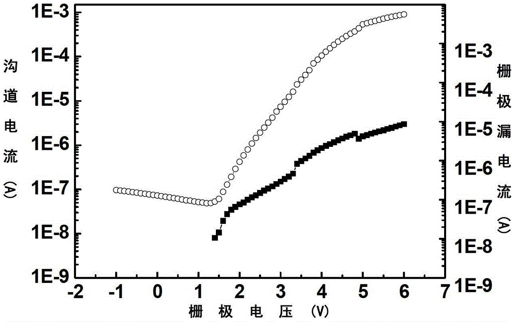
[0079] Aluminum oxide thin film performance test results:
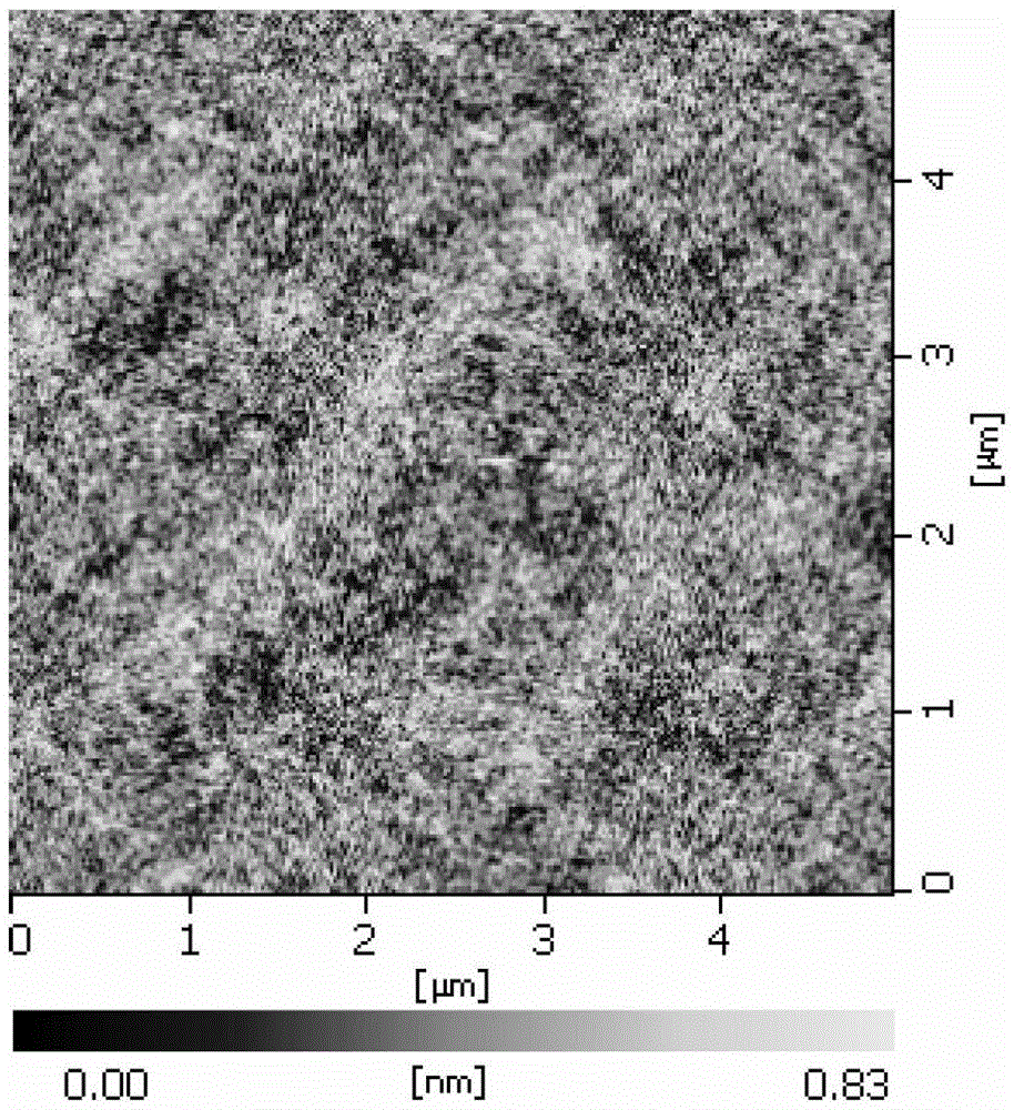
[0080] The 80nm aluminum oxide thin film prepared by spin coating method was used to measure its morphology (AFM image, the side length is 5 microns). Such as Figure 4 shown. The surface of the film is relatively flat, the roughness has increased, and there are...
Embodiment 1-2
[0087] The preparation method of aluminum oxide thin film, comprises the following steps:
[0088] Monoethanolamine and butanediol monomethyl ether are used as stabilizers, and the molar ratio of aluminum nitrate to monoethanolamine and butanediol monomethyl ether is 1:2:1. The remaining steps are the same as implementation 1.
[0089] A thin film transistor is prepared, comprising the following steps:
[0090] With embodiment 1.
[0091] Aluminum oxide thin film performance test results:
[0092] The 80nm aluminum oxide thin film prepared by spin coating method was used to measure its morphology (AFM image, the side length is 5 microns). The characterization parameters are as follows:
[0093] Scanning area: 5μm×5μm
[0094] Film valley value (P-V value) is 2.1nm
[0095] The root mean square roughness value (RMS value) is 0.11nm
[0096] Using the frequency-capacitance method, the dielectric constant is measured and calculated on an impedance meter to obtain a dielect...
PUM
| Property | Measurement | Unit |
|---|---|---|
| softening point | aaaaa | aaaaa |
| softening point | aaaaa | aaaaa |
Abstract
Description
Claims
Application Information
 - R&D
- Intellectual Property
- Life Sciences
- Materials
- Tech Scout
- Unparalleled Data Quality
- Higher Quality Content
- 60% Fewer Hallucinations
Browse by: Latest US Patents, China's latest patents, Technical Efficacy Thesaurus, Application Domain, Technology Topic, Popular Technical Reports.
© 2025 PatSnap. All rights reserved.Legal|Privacy policy|Modern Slavery Act Transparency Statement|Sitemap|About US| Contact US: help@patsnap.com


