Texture surface making treatment method for silicon wafer

A processing method and technology of silicon wafers, applied in the direction of final product manufacturing, sustainable manufacturing/processing, electrical components, etc., can solve the problems of reducing production efficiency and achieve the effect of avoiding leakage

Active Publication Date: 2012-12-12
BEIJING NAURA MICROELECTRONICS EQUIP CO LTD
View PDF4 Cites 6 Cited by
  • Summary
  • Abstract
  • Description
  • Claims
  • Application Information

AI Technical Summary

Problems solved by technology

However, compared with the conventional dry texturing process, the depth of the suede surface obtained by the improved method is not much different, but the size is above 0.5um and the angle is below 50 degrees, so the effect of anti-reflection is compromised
In addition, the introduction of C-containing gas also forms a pollution source, requiring frequent opening of the chamber for maintenance, reducing production efficiency

Method used


Image

  • Texture surface making treatment method for silicon wafer
  • Texture surface making treatment method for silicon wafer
  • Texture surface making treatment method for silicon wafer

Examples


example 1

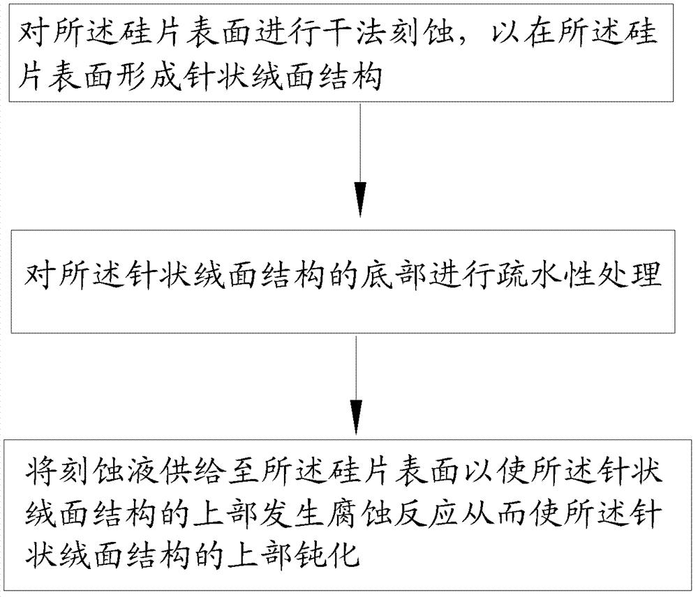
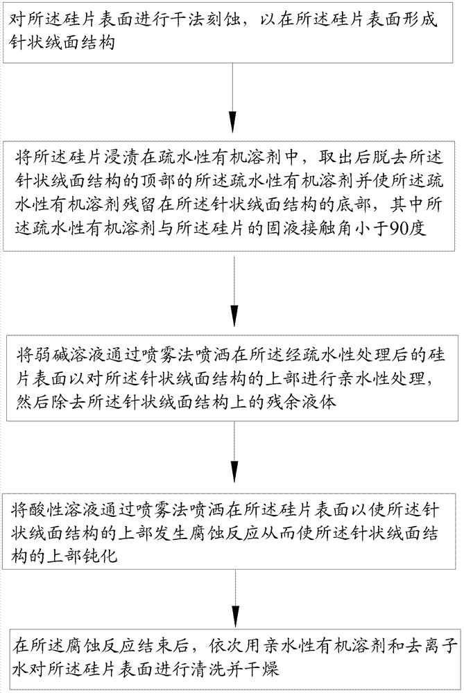
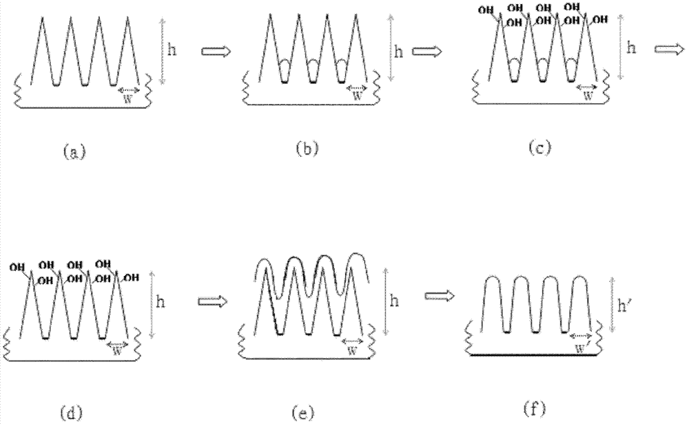
[0074] 1) Use Cl 2 , SF 6 , O 2 , Ar and other gases to etch the surface of the silicon wafer. At the same time, the ratio of various gases can be controlled, such as image 3 As shown in (a), an acicular suede structure with a depth h of 1 μm and a width w of 0.3 μm is formed, and the apex of the acicular suede is sharp.

[0075] 2) Hydrophobic treatment is performed on the bottom of the needle-like suede structure.

[0076] Next, the silicon wafer is immersed in hexane, and after taking it out, it is centrifugally dried at a speed below 1500RPM, such as image 3 As shown in (b), hexane remains at the bottom of the needle-like suede structure.

[0077] 3) supplying an etchant to the surface of the silicon wafer to cause a corrosion reaction on the upper portion of the needle-shaped textured structure to passivate the upper portion of the needle-shaped textured structure.

[0078] Firstly, the mixed solution of ammonia water and hydrogen peroxide is sprayed on the surface...


PUM


Abstract

The invention discloses a texture surface making treatment method for a silicon wafer. The texture surface making treatment method includes steps of 1), performing dry etching for the surface of the silicon wafer so as to form a needle-shaped texture surface structure on the surface of the silicon wafer; 2), performing hydrophobic treatment for the bottom of the needle-shaped texture surface structure; and 3), supplying etching liquid to the surface of the silicon wafer so that the upper portion of the needle-shaped texture surface structure is subjected to corrosion reaction and is passivated. The texture surface making treatment method for the silicon wafer in an embodiment of the invention has the advantages that the top of the needle-shaped texture surface structure can be passivated on the premise that the size and the angle of the needle-shaped texture surface structure are maintained, so that an anti-reflection effect of the texture surface structure can be guaranteed, the needle-shaped texture surface structure can also be prevented from being broken in a follow-up screen printing process for an electrode, and electric leakage can be avoided.

Description

technical field [0001] The invention relates to a texturing treatment method for silicon wafers. Background technique [0002] After the oil crisis in the 1970s, people began to pay attention to the application of new energy sources such as solar energy. Since the beginning of this century, the production of solar cells has grown at an alarming rate every year, especially crystalline silicon cells. [0003] The production process of traditional crystalline silicon cells includes incoming cleaning, texturing, diffusion, secondary cleaning to remove phosphorus silicon, anti-reflection coating, printing metal wires, drying and sintering, efficiency sorting and other steps. The main purpose of texturing is to form a rough microstructure on the smooth silicon wafer surface to reduce the specular reflection of light, thereby enhancing the diffuse reflection to play the role of light trapping, and on the other hand, to increase the contact area of ​​the PN junction so as to be eff...

Claims


Application Information

Patent Timeline
Patent Type & Authority Applications(China)
IPC IPC(8): H01L31/18
CPCY02P70/50
Inventor 白志民
Owner BEIJING NAURA MICROELECTRONICS EQUIP CO LTD
Why Eureka
Try Eureka