A kind of patterned electrode, preparation method and organic solar cell
A solar cell and patterning technology, applied in circuits, photovoltaic power generation, electrical components, etc., can solve the problems that organic solar cells cannot be prepared in a large area, the preparation process is complicated, and the cost is expensive.
- Summary
- Abstract
- Description
- Claims
- Application Information
AI Technical Summary
Problems solved by technology
Method used
Image
Examples
Embodiment 1
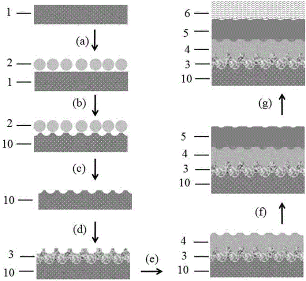
[0068]The ITO electrode 1 is ultrasonically cleaned with detergent plus deionized water and acetone in sequence, and then the ITO electrode 1 is treated with ultraviolet light. Then if Figure 4 As shown, perform the following steps:
[0069] (a) On the ITO electrode 1, PS nanospheres with a size of 100 nm are prepared as a nanostructure layer 2 (such as Figure 5 as shown in a);
[0070] (b) Using PS nanospheres as a template, corrode the ITO electrode 1 with hydrochloric acid, and rinse off the residual hydrochloric acid on the electrodes and nanospheres with deionized water after 2.5 minutes of corrosion;
[0071] (c) Remove the PS nanospheres with ultrasound in chloroform, then ultrasonically clean them in isopropanol for 15 minutes, and dry them with nitrogen to obtain a patterned ITO electrode 10 (such as Figure 5 as mentioned in b);
[0072] (d) Prepare 10nm thick MoO on the patterned ITO electrode 10 by thermal evaporation method 3 As the anode buffer layer as th...
Embodiment 2
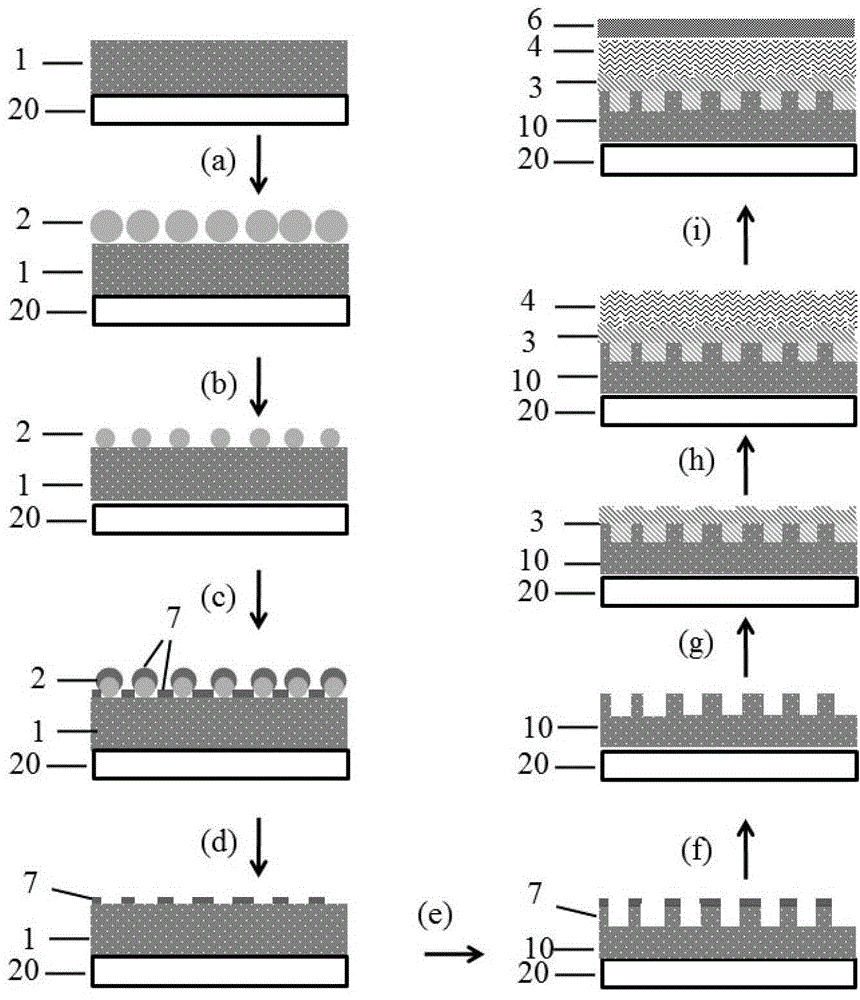
[0080] The ITO electrode 1 is ultrasonically cleaned with detergent plus deionized water and acetone in sequence, and then the ITO electrode 1 is treated with ultraviolet light. Then carry out the following steps to prepare the patterned electrode 10:
[0081] (a) Spin-coating method (2500rpm, 30s) on the ITO electrode 1 to prepare SiO with a size of 200nm 2 Nanospheres as nanostructures 2;
[0082] (b) Due to the conditions of (a), SiO prepared on ITO 2 Nanospheres are not SiO forming close contacts 2 Nanosphere layer, but there is a larger gap between the nanosphere and the nanosphere, so it is not necessary to reduce the size of the nanosphere ( figure 2 In (b) step), it can be prepared in SiO 2 After the nanospheres, the SiO 2 Nanospheres are used as templates to prepare metal thin film layers;
[0083] (c) Using magnetron sputtering method to SiO 2 The nanosphere is used as a template to prepare a Cr layer with a thickness of 150 nm on the ITO electrode 1 as the m...
PUM
| Property | Measurement | Unit |
|---|---|---|
| thickness | aaaaa | aaaaa |
| size | aaaaa | aaaaa |
| size | aaaaa | aaaaa |
Abstract
Description
Claims
Application Information


