

Silicon single crystal rod
A single crystal silicon rod, silicon rod technology, applied in the direction of single crystal growth, single crystal growth, crystal growth, etc., can solve the problems of wafer abrasive crushing, disconnection, lifting, etc., to improve the yield and reduce the disconnection rate. Effect
Inactive Publication Date: 2012-12-26
JIANGSU SHUNDA SEMICON DEV
View PDF0 Cites 7 Cited by
- Summary
- Abstract
- Description
- Claims
- Application Information
AI Technical Summary
Problems solved by technology
Because the thickness of the wafer itself is very thin and the material is very brittle, the wafers at both ends of the crystal rod and the wafers at the butt joint are easily crushed by the abrasive; in addition, the debris generated during the cutting process will directly fall onto the wire mesh, causing the wire to break. This greatly increases the chances of
Method used
View moreImage
Smart ImageViewing Examples

Examples
Embodiment Construction
[0011] The present invention will be further described below in conjunction with the accompanying drawings.
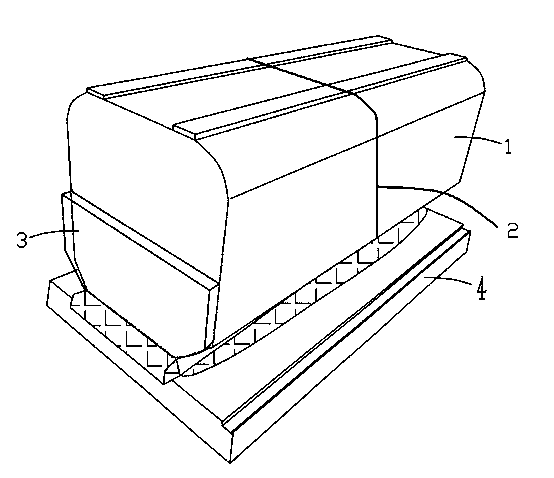
[0012] as attached figure 1 Shown is a 12-inch single crystal silicon rod, the single crystal silicon rod is connected together by more than two silicon rod bodies 1 through the end surface sticking layer 2, and its bottom is stuck on the base 4 by epoxy resin, on the silicon rod The front and rear ends of the rod body 1 are provided with baffles 3, and the baffles 3 are made of resin, and are all adhered to the silicon rod body 1 by epoxy resin.
Login to View More PUM
 Abstract
The invention discloses a silicon single crystal rod. More than two silicon rod bodies are connected together through an end surface adhesion layer; the bottoms of the silicon rod bodies are adhered to a base through epoxy resin; baffles are arranged at the front end and the back end of each silicon rod body; the baffles are made of resin; and the baffles are all adhered to the silicon rod bodies through epoxy resin. According to the silicon single crystal rod provided by the invention, the fixed connection between the baffles at the two ends of each silicon rod body and monomers can protect the contact surfaces between chips at the two ends of each silicon rod body and the monomers in a cutting process, so that the yield is improved; and debris generated by butt end surfaces in the cutting process cannot fall down, so that the disconnection rate is reduced.
Description
[0001] technical field [0002] The invention relates to a single crystal silicon rod. Background technique [0003] Single crystal silicon rod is a single crystal of silicon, a crystal with a basically complete lattice structure, different directions have different properties, and is a good semiconductor material. Single crystal silicon has the physical properties of metalloid and has weak conductivity. Its conductivity increases with the increase of temperature, and it has significant semiconductivity. Doping a small amount of group IIIA elements, such as boron, in ultra-pure single crystal silicon can increase its conductivity and form a P-type silicon semiconductor; if doping a small amount of group VA elements, such as phosphorus or arsenic, can improve the degree of conductivity , forming an N-type silicon semiconductor. [0004] During the wire cutting of single crystal silicon rods, the steel wire with liquid abrasive impacts the wafer at a linear speed of more tha...
Claims
Login to View More Application Information
Patent Timeline
 Patent Type & AuthorityApplications(China)
IPC IPC(8): C30B29/06C30B33/06B28D5/00B28D7/04
Inventor倪云达葛正芳钱大丰
OwnerJIANGSU SHUNDA SEMICON DEV