Method for realizing all-fiber package of semiconductor saturable absorption mirror

A saturable absorption and semiconductor technology, applied in the direction of lasers, laser components, electrical components, etc., can solve the problems of complex structure, low price, and high price, and achieve the effect of good repeatability, simple operation, and easy access

Inactive Publication Date: 2012-12-26
NAT UNIV OF DEFENSE TECH
View PDF1 Cites 8 Cited by
  • Summary
  • Abstract
  • Description
  • Claims
  • Application Information

AI Technical Summary

Problems solved by technology

[0006] The semiconductor saturable absorber mirror packaged with a copper base is cheap, and the semiconductor saturable absorber mirror has a large area, which can provide multiple chances of damage; but it is used in a passive mode-locked fiber laser. Two precise three-dimensional adjustment brackets are required for the fiber respectively. The semiconductor saturable absorbing m

Method used


Image

  • Method for realizing all-fiber package of semiconductor saturable absorption mirror
  • Method for realizing all-fiber package of semiconductor saturable absorption mirror
  • Method for realizing all-fiber package of semiconductor saturable absorption mirror

Examples


Embodiment Construction

[0027] Below in conjunction with accompanying drawing and specific example the present invention will be further described:

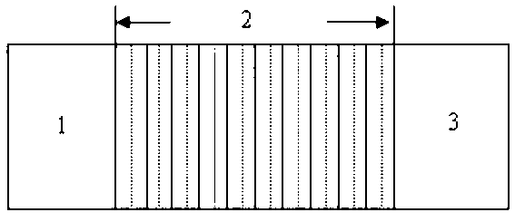
[0028] figure 1 Shown are the structure and plan views of the unpackaged semiconductor saturable absorber mirror 4 . Such as figure 1 As shown, an unpackaged semiconductor saturable absorbing mirror 4 is made of gallium arsenide substrate 1, and several layers of aluminum arsenide and gallium arsenide or aluminum arsenide potassium and aluminum arsenide are alternately grown. The effect is similar to that of a Bragg reflection grating mirror 2 and a semiconductor saturable absorber 3 composed of a multi-quantum well structure.

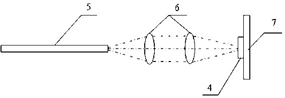
[0029] figure 2 Shown is a schematic diagram of the coupling system of a semiconductor saturable absorbing mirror packaged with a copper base and an optical fiber. Such as figure 2 As shown, the semiconductor saturable absorbing mirror 4 is pasted on the copper base 7, and the copper base 7 and the optical fiber 5 are res...


PUM


Abstract

The invention discloses a method for realizing an all-fiber package of a semiconductor saturable absorption mirror. The method comprises the following steps of: uniformly spreading ultraviolet glue on the upper surface of a ceramic fiber pin except for the part of the head face of a fiber core; slowly placing a semiconductor saturable absorption mirror which is not packaged on the upper surface of the ceramic fiber pin of a fiber ferrule connector (FC) joint horizontally; and connecting a fiber at the other end of the fiber FC joint in a cavity of a fiber laser. The semiconductor saturable absorption mirror or the fiber FC joint can be changed when experiments show that parameters of the placed semiconductor saturable absorption mirror of the model fail to satisfy the experiment requirements or show that the head face of a fiber core corresponding to the semiconductor saturable absorption mirror is damaged in the experiment process; and the ultraviolet glue can be adopted to cure when the experiments provs that the various parameters of the semiconductor saturable absorption mirror are accordant with the requirements. The method provided by the invention breaks through the technological monopoly at home and abroad, and is simple in operation, low in cost and excellent in repeatability; and the method fills the blank in the technical field at home.

Description

technical field [0001] The invention relates to an all-fiber laser based on a semiconductor saturable absorption mirror, in particular to a method for realizing all-fiber packaging of a semiconductor saturable absorption mirror. Background technique [0002] A passively mode-locked fiber laser based on a semiconductor saturable absorber mirror can generate picosecond (10 -12 seconds) to femtoseconds (10 -15 second) level ultrashort pulse, ultrashort pulse technology is an important means to study the microcosm and reveal new ultrafast processes in physics, chemistry, biology, optoelectronics, and laser spectroscopy. One of the necessary conditions for optical communication systems. Ultrashort pulse technology also has broad application prospects in the fields of industrial processing, medicine, optical information processing, full-color display and laser printing. Semiconductor saturable absorber mirror is an important mode-locking device for passively mode-locked fiber l...

Claims


Application Information

Patent Timeline
IPC IPC(8): H01S3/098
Inventor 宋锐王彦斌陈胜平侯静程金龙陆启生
Owner NAT UNIV OF DEFENSE TECH
Why Eureka
Try Eureka