Single chip integrated optical matrix-vector multiplier

A technology of monolithic integration and vector multiplication, which is applied in the direction of instruments, complex mathematical operations, and logic circuits using optoelectronic devices, etc., can solve the problems of large power consumption, limitation, and large size, and reduce power consumption and cost, and reduce The effect of silicon-based size and good scalability

Inactive Publication Date: 2013-01-09
TSINGHUA UNIV +1
View PDF5 Cites 32 Cited by
  • Summary
  • Abstract
  • Description
  • Claims
  • Application Information

AI Technical Summary

Problems solved by technology

Due to the requirements of data capacity and real-time performance, massive data processing usually adopts distributed processing and parallel processing. The distributed processing is ultimately limited by the processing capability of the hardware. The further reduction of circuit line width is limited by the quantum tunneling effect and power consumption, which makes it difficult to greatly improve the performance of electronic mass data processing
Therefore, the parallel processing of massive data in electronics will be difficult to meet the explosive growth of massive data processing requirements
[0003] The photonics data processing method provides the possibility to greatly improve the performance of massive data processing. Most methods of digital signal processing ultimately involve matrix operations. Due to the characteristics of high bandwidth and parallel processing of optical signals, it just meets the requirements of matrix operations. , traditional optical matrix operations such as Stanford multipliers (J.W.Goodman, A.Dias, and L.Woody, Fully parallel, high-speed incoherent optical method for performing discrete Fourier transforms. Optics letters, 1978.2(1): p.1-3 .) Although this kind of multiplier can improve the calculation speed, it needs to be realized by bulk optical elements such as lenses, and the structure is complex, the size is large, and the price is expensive
[0004] In recent years, the rapid development of silicon-based micro-nano photonics has made it possible to realize monolithic integrated optical matrix-vector multipliers. In the prior art, the loading of multi-wavelength light sources and optical information on silicon-based is generally achieved by modulating multiple discrete semiconductors. The laser is realized, and then the optical signals of each wavelength are combined into the same waveguide through WDM (Wavelength Division Multiplexer). Developing a compact multi-wavelength light source and performing wavelength-selective modulation to obtain a monolithic integrated matrix-vector multiplier with a simpler structure will have great significance for massive data processing

Method used


Image

  • Single chip integrated optical matrix-vector multiplier
  • Single chip integrated optical matrix-vector multiplier
  • Single chip integrated optical matrix-vector multiplier

Examples


Embodiment Construction

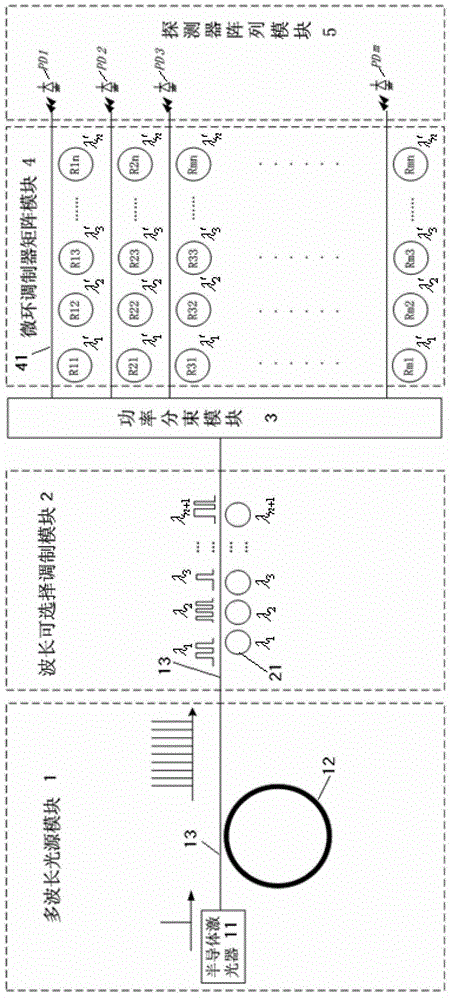
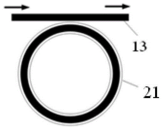
[0015] The present invention will be described in detail below in conjunction with the accompanying drawings and embodiments.

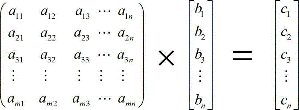
[0016] The principle of matrix-vector multiplication is to realize the multiplication operation between an input vector b and an input matrix a, and obtain an output vector c. The specific calculation formula is:

[0017] a 11 a 12 a 13 . . . a 1 n a 21 a ...


PUM

PropertyMeasurementUnit
diameteraaaaaaaaaa

Abstract

The invention relates to a single chip integrated optical matrix-vector multiplier which is characterized by comprising a silicon base, wherein a multi-wavelength light source module, a wavelength selecting modulating module, a power beam splitting module, a micro-ring modulator matrix module and a detector array module are integrated on the silicon base; the multi-wavelength light source module is used for outputting multi-wavelength optical signals with n+1different wavelengths to the wavelength selecting modulating module; the wavelength selecting modulating module is used for selectively modulating each wavelength optical signal in the multi-wavelength optical signals and then sending to the power beam splitting module; the power beam splitting module is used for performing 1:m equal power beam splitting on the multi-wavelength optical signals and sending the multi-wavelength optical signals after being subjected to the beam splitting to the micro-ring modulator matrix module; the micro-ring modulator matrix module is used for processing m paths of multi-wavelength optical signals and sending a processing result to the detector array module; and the detector array module is used for detecting the outputted optical signals. The single chip integrated optical matrix-vector multiplier can be widely applied to the processing process of mass data.

Description

technical field [0001] The invention relates to an optical massive data operation system, in particular to a single-chip integrated optical matrix-vector multiplier. Background technique [0002] With the development of information technology, massive amounts of data need to be processed at any time in areas involving the national economy and the people's livelihood, such as password deciphering, video surveillance, DNA information analysis and new drug development, photoelectric countermeasures, and climate monitoring. Due to the requirements of data capacity and real-time performance, massive data processing usually adopts distributed processing and parallel processing. The distributed processing is ultimately limited by the processing capability of the hardware. The further reduction of circuit line width is limited by the quantum tunneling effect and power consumption, which makes it difficult to greatly improve the performance of electronic mass data processing. Theref...

Claims


Application Information

Patent Timeline
Patent Type & Authority Applications(China)
IPC IPC(8): G06F7/523G06F17/16G02F3/00
Inventor 鲍成英杨林杨昌喜
Owner TSINGHUA UNIV
Why Eureka
Try Eureka