Insulating layer of flexible film transistor and preparation method thereof

A flexible thin film and transistor technology, applied in the manufacture of semiconductor/solid state devices, electric solid state devices, semiconductor devices, etc., can solve the problem of incompatibility with flexible substrates, no insulating layer materials for flexible thin film transistors, and insufficient insulating layer materials. attention and other issues, to achieve the effect of good insulation performance and electrical strength, good insulation performance and cost saving

Inactive Publication Date: 2013-01-23
SHANGHAI JIAO TONG UNIV
View PDF3 Cites 1 Cited by
  • Summary
  • Abstract
  • Description
  • Claims
  • Application Information

AI Technical Summary

Problems solved by technology

Semiconductor materials have achieved good development in recent years. The mobility of solution-processable organic semiconductors and metal oxide semiconductor materials has far exceeded that of traditional amorphous silicon. However, relatively speaking, insulating materials with the same importance layer materials have not received enough attention, and there are not enough insulating layer materials that can be applied to the actual production of flexible thin film transistors.
Materials for traditional insulating layers, such as chemical vapor deposited silicon nitride, usually require a high temperature of at least 300 degrees Celsius and cannot be compatible with general flexible substrates. However, the insulating layer processed by the solution method at this stage is comparable to traditional vacuum in terms of process control and dielectric strength. There is still a big gap in the insulating layer processed by the process

Method used


Image

  • Insulating layer of flexible film transistor and preparation method thereof
  • Insulating layer of flexible film transistor and preparation method thereof

Examples


Embodiment Construction

[0023] Embodiments of the present invention will be further described below in conjunction with the accompanying drawings.

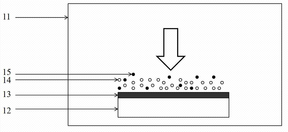
[0024] The insulating layer of the present invention is one of the components of the flexible thin film transistor, please refer to figure 1 , the insulating layer 13 of the flexible thin film transistor shown in the figure is located on the substrate 12, and the substrate 12 is located at the bottom layer of the flexible thin film transistor. In the structure thin film transistor is a flexible substrate that has prepared source electrodes, drain electrodes and semiconductor layers.

[0025] The insulating layer 13 of the flexible thin film transistor of the present invention is a thin film of a hydrocarbon polymer formed by a plasma-enhanced chemical vapor deposition (PECVD) process on the substrate 12, and the hydrocarbon polymer refers to a diamond-like amorphous hydrocarbon polymer.

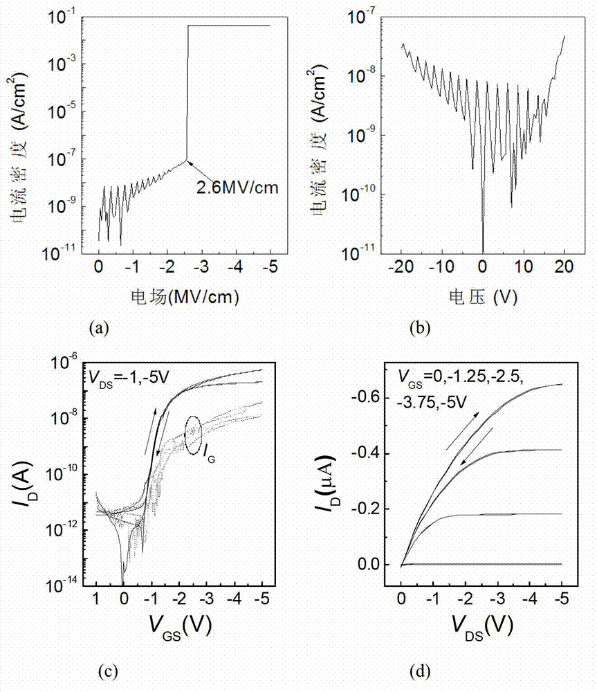
[0026] The preparation method for the insulating layer of the fl...


PUM


Abstract

The invention discloses an insulating layer of a flexible film transistor and a preparation method of the insulating layer. The insulating layer of the flexible film transistor is a film of hydrocarbon-based polymer formed on a substrate. The preparation method of the insulating layer adopts hydrogen and acetylene gas as raw materials. Under the conditions of room temperature and vacuum, the film of hydrocarbon-based polymer is deposited on the substrate in a plasma enhanced chemical vapor deposition (PECVD) system so as to finish the preparation of the insulating layer of the flexible film transistor. The insulating layer disclosed by the invention has the advantages of good insulating performance and higher electric breakdown strength. Under the condition of room temperature, the preparation method enables the insulating layer to be well compatible with the flexible substrate. The insulating layer can be processed by adopting the PECVD process. The preparation method disclosed by the invention can be used for preparing the flexible film transistor, so as to further promote the development of flexible electron.

Description

technical field [0001] The invention relates to an electronic device, in particular to an insulating layer of a flexible thin film transistor and a preparation method thereof, belonging to the technical field of flexible electronics. Background technique [0002] Thin film transistors based on hydrogenated amorphous silicon semiconductors have been widely used in technical fields such as liquid crystal displays. In recent years, with the continuous development of various new semiconductor materials, the performance of organic thin film transistors and metal oxide transistors has caught up with or even surpassed that of traditional amorphous silicon thin film transistors, and the recent rapid development of emerging technologies, such as solution processing technology The thin film transistor can be integrated with the flexible substrate at low cost, further expanding the application range of the thin film transistor. With people's increasing requirements for low cost and po...

Claims


Application Information

Patent Timeline
Patent Type & Authority Applications(China)
IPC IPC(8): H01L51/05H01L51/30H01L51/40
Inventor 冯林润唐伟陈苏杰徐小丽郭小军
Owner SHANGHAI JIAO TONG UNIV
Why Eureka
Try Eureka