Junctionless silicon nanowire transistor based on bulk-silicon material and method for manufacturing junctionless silicon nanowire transistor

A silicon nanowire and silicon material technology is applied in the field of junction-free silicon nanowire transistors and their preparation to achieve the effects of realizing source-drain contact resistance, realizing integration, and small source-drain contact resistance

Inactive Publication Date: 2013-02-06
INST OF SEMICONDUCTORS - CHINESE ACAD OF SCI
View PDF6 Cites 21 Cited by
  • Summary
  • Abstract
  • Description
  • Claims
  • Application Information

AI Technical Summary

Problems solved by technology

At present, many research groups have successfully realized junction-free silicon nanowire transistors on silicon-on-insulator (SOI) substrates, which can achieve comparable or even better performance than traditional inversion-mode field-effect transistors, which is of great research value, but based on Junction-free silicon nanowire transistors from bulk silicon have not yet been reported

Method used


Image

  • Junctionless silicon nanowire transistor based on bulk-silicon material and method for manufacturing junctionless silicon nanowire transistor
  • Junctionless silicon nanowire transistor based on bulk-silicon material and method for manufacturing junctionless silicon nanowire transistor
  • Junctionless silicon nanowire transistor based on bulk-silicon material and method for manufacturing junctionless silicon nanowire transistor

Examples


Embodiment Construction

[0045] In order to make the object, technical solution and advantages of the present invention clearer, the present invention will be described in further detail below in conjunction with specific embodiments and with reference to the accompanying drawings.

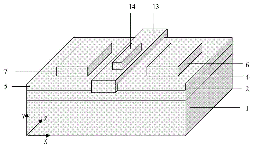
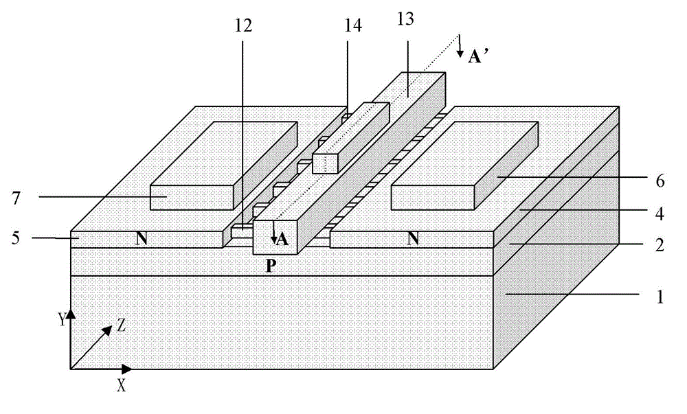
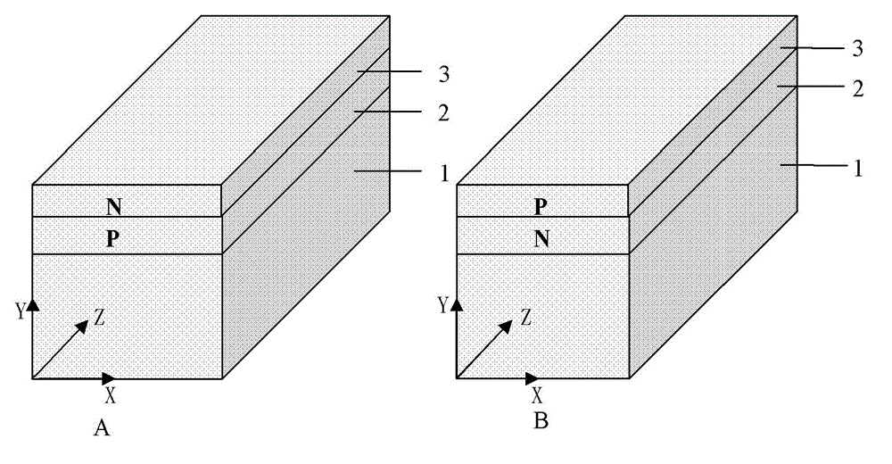
[0046] see Figure 1 to Figure 6 As shown, the junction-free silicon nanowire transistor based on bulk silicon material provided by the present invention includes: an integral silicon substrate 1; a first doped layer 2, which is formed on the bulk silicon by ion implantation The upper part of the substrate 1, and the doping type of the first doped layer 2 is P-type or N-type; a second doped layer 3, the second doped layer 3 is formed on the bulk silicon substrate by ion implantation 1, and located on the first doped layer 2, the doping type of the second doped layer 3 is opposite to that of the first doped layer 2, and different types of doped layers form a PN junction Play the role of electrical isolation; a source regi...


PUM

PropertyMeasurementUnit
thicknessaaaaaaaaaa
lengthaaaaaaaaaa
widthaaaaaaaaaa

Abstract

The invention discloses a junctionless silicon nanowire transistor based on a bulk-silicon material and a method for manufacturing the junctionless silicon nanowire transistor. The junctionless silicon nanowire transistor comprises a bulk-silicon substrate, a polycrystalline grid, a drain electrode, a source electrode and a grid electrode, a P-type doped layer or an N-type doped layer is manufactured on the bulk-silicon substrate, an N-type doped layer or a P-type doped layer with a doping type opposite to the first P-type doped layer or first the N-type doped layer is manufactured on the first P-type doped layer or the first N-type doped layer, and a PN junction is formed by the different types of doped layers and realizes an electric isolation effect; a source region, a drain region and a silicon nanowire are manufactured on the second N-type doped layer or the second P-type doped layer, and the source region and the drain region are connected with each other by the silicon nanowire to form conducting channels; an insulating dielectric layer is manufactured on the surface of the integral silicon nanowire, the surface of the source region and the surface of the drain region; the polycrystalline grid is manufactured between the source region and the drain region and completely wraps the silicon nanowire; the drain electrode is manufactured on the drain region of silicon; the source electrode is manufactured on the source region of the silicon; and the grid electrode is manufactured on the polycrystalline grid. The junctionless silicon nanowire transistor and the method have the advantage that the junctionless silicon nanowire transistor can be manufactured on the bulk-silicon substrate.

Description

technical field [0001] The invention relates to the technical field of manufacturing semiconductor devices, in particular to a junction-free silicon nanowire transistor based on bulk silicon material and a preparation method thereof. Background technique [0002] With the continuous improvement of integrated circuit manufacturing technology, the current metal-oxide-semiconductor field effect transistor (MOSFET) technology node has entered 22nm, and the physical gate length of the device has been smaller than 20nm. As the device size continues to shrink, the primary problem it faces is that it is increasingly affected by the short-channel effect. [0003] Because silicon nanowire transistors can control the channel from multiple directions, they can effectively suppress the short-channel effect. Therefore, it is expected to solve the increasingly serious problem of the short-channel effect and enable the device size to continue to be reduced. However, for traditional inversi...

Claims


Application Information

Patent Timeline
Patent Type & Authority Applications(China)
IPC IPC(8): H01L29/78H01L29/10H01L21/336
Inventor 李小明韩伟华张严波颜伟杜彦东陈燕坤杨富华
Owner INST OF SEMICONDUCTORS - CHINESE ACAD OF SCI
Why Eureka
Try Eureka