

A method of making non-absorbing window of Gaas-based semiconductor laser
A laser and semiconductor technology, applied in the direction of semiconductor lasers, lasers, laser parts, etc., can solve the problems of limited application, low yield, increased process cost and complexity, etc., to suppress output light absorption, stabilize emission wavelength, reduce Effect of Effective Refractive Index
- Summary
- Abstract
- Description
- Claims
- Application Information
AI Technical Summary
Problems solved by technology
Method used
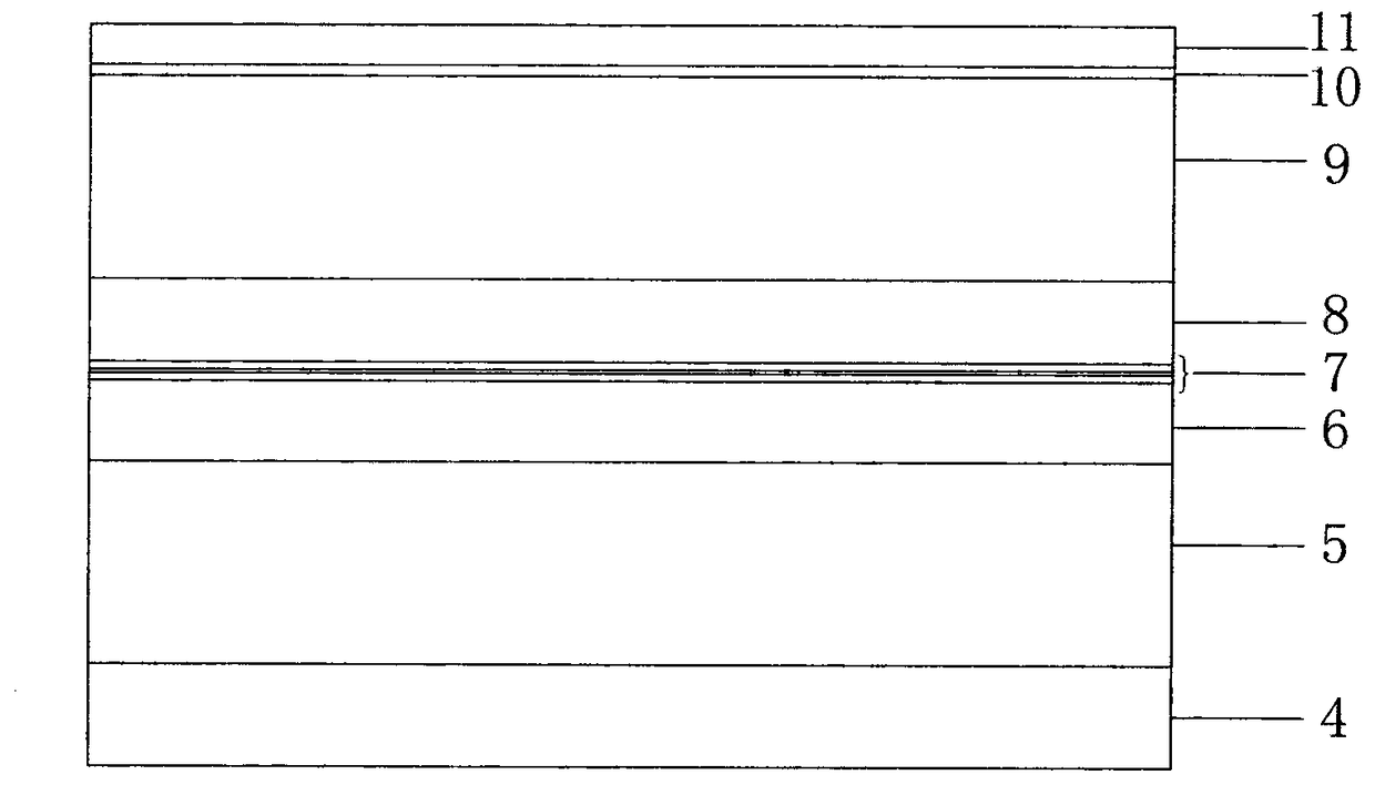
Image

Examples
Embodiment Construction
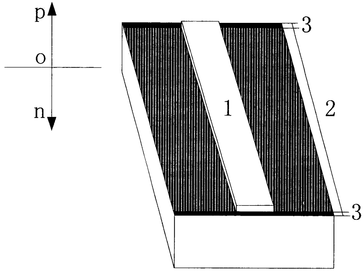
[0010] 1. After cleaning the laser epitaxial wafer, use the method of electron beam evaporation to evaporate SiO with a thickness of 0.5-1.2 microns 2 .
[0011] 2. After the photoresist-coated epitaxial wafer is exposed and developed by photolithography, the SiO on the region (1) 2 are protected by photoresist, while other regions on the SiO 2 bare.
[0012] 3. Use hydrofluoric acid solution (the volume ratio of hydrofluoric acid to water is 1:20) and phosphoric acid solution to corrode the exposed SiO successively 2 And the lower GaAs ohmic contact layer, etch out the laser bar structure.
[0013] 4. Evaporate TiO with a thickness of 0.7-1.8 microns on the surface of the laser epitaxial wafer by electron beam evaporation 2 , followed by hot acetone combined with ultrasonic process to remove the photoresist and the TiO on it 2 , such that region (1) consists of SiO 2 +Photoresist+TiO 2 The structure becomes monolayer SiO 2 structure, while regions (2), (3) are mono...
PUM
 Abstract
Description
Claims
Application Information