Flat spectrum absorption layer for detectors and manufacture method thereof

An absorption layer and detector technology, which is applied to the absorption layer for a detector with a flat spectrum and the field of its preparation, can solve the problems of difficulty in using line array and area array detectors, weak adhesion of the infrared absorption layer, and incompatibility of processes, etc. Excellent heat transfer performance, small specific heat capacity, and firm adhesion

Inactive Publication Date: 2013-02-13
SHANGHAI INST OF TECHNICAL PHYSICS - CHINESE ACAD OF SCI
View PDF3 Cites 3 Cited by
  • Summary
  • Abstract
  • Description
  • Claims
  • Application Information

AI Technical Summary

Problems solved by technology

Solve the problem that the infrared absorption layer of the uncooled infrared detector is not firmly attached or the absorption band is narrow, it is not compatible with the standard semiconductor process, and it is difficult to be used in line array and area array detectors

Method used


Image

  • Flat spectrum absorption layer for detectors and manufacture method thereof

Examples


example 1

[0021] Based on Mn-(1-x)Pb(Mg 1 / 3 Nb 2 / 3 )O 3 -xPbTiO 3 In the 128×1 pyroelectric array detector made of (Mn-PMNT) material, the flat wide spectrum absorption structure design provided by the present invention is adopted. Specifically, it is realized through the following steps.

[0022] (1) Mn-PMNT surface treatment

[0023] 1) Clean the Mn-PMNT wafer polarized in the direction. Mechanical thinning, flattening and polishing of the A-side of the Mn-PMNT wafer. Wet etch the A side of the Mn-PMNT wafer to remove defects and damage.

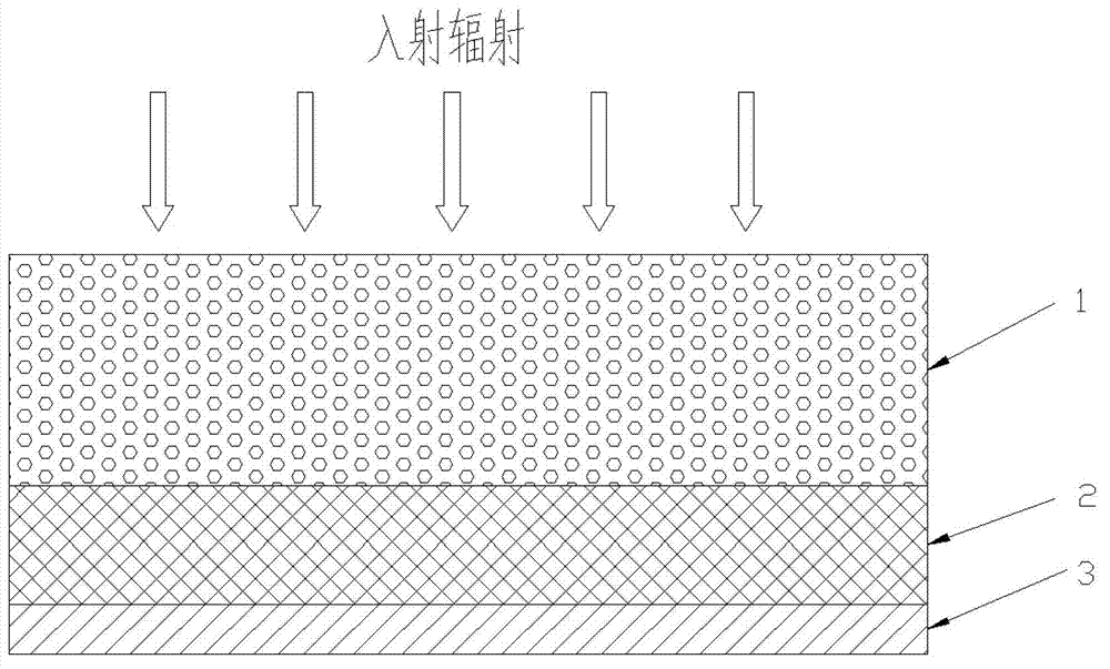
[0024] (2) Deposit the infrared absorbing layer and etch to form the electrode structure

[0025] 2) cleaning the Mn-PMNT wafer, and photolithography patterning on the A side.

[0026] 3) Depositing a chromium metal film and a nickel metal film on the A side of the Mn-PMNT wafer by ion beam sputtering. Float cleaning. Among them, the thickness of the chromium metal film is 18nm, and the thickness of the nickel metal film is 75nm.

[0027...

example 2

[0032] Based on Mn-(1-x)Pb(Mg 1 / 3 Nb 2 / 3 )O 3 -xPbTiO 3 In the 128×1 pyroelectric array detector made of (Mn-PMNT) material, the flat wide spectrum absorption structure design provided by the present invention is adopted. Specifically, it is realized through the following steps.

[0033] (1) Mn-PMNT surface treatment

[0034] 1) Clean the Mn-PMNT wafer polarized in the direction. Mechanical thinning, flattening and polishing of the A-side of the Mn-PMNT wafer. Wet etch the A side of the Mn-PMNT wafer to remove defects and damage.

[0035] (2) Deposit the infrared absorbing layer and etch to form the electrode structure

[0036] 2) cleaning the Mn-PMNT wafer, and photolithography patterning on the A side.

[0037] 3) Depositing a chromium metal film and a nickel metal film on the A side of the Mn-PMNT wafer by ion beam sputtering. Float cleaning. The thickness of the chromium metal film is 20nm, and the thickness of the nickel metal film is 80nm.

[0038] 4) Photoli...

example 3

[0043] Based on Mn-(1-x)Pb(Mg 1 / 3 Nb 2 / 3 )O 3 -xPbTiO 3 In the 128×1 pyroelectric array detector made of (Mn-PMNT) material, the flat wide spectrum absorption structure design provided by the present invention is adopted. Specifically, it is realized through the following steps.

[0044] (1) Mn-PMNT surface treatment

[0045] 1) Clean the Mn-PMNT wafer polarized in the direction. Mechanical thinning, flattening and polishing of the A-side of the Mn-PMNT wafer. Wet etch the A side of the Mn-PMNT wafer to remove defects and damage.

[0046] (2) Deposit the infrared absorbing layer and etch to form the electrode structure

[0047] 2) cleaning the Mn-PMNT wafer, and photolithography patterning on the A side.

[0048] 3) Depositing a chromium metal film and a nickel metal film on the A side of the Mn-PMNT wafer by ion beam sputtering. Float cleaning. Among them, the thickness of the chromium metal film is 22nm, and the thickness of the nickel metal film is 85nm.

[0049...


PUM

PropertyMeasurementUnit
thicknessaaaaaaaaaa
thicknessaaaaaaaaaa
thicknessaaaaaaaaaa

Abstract

The invention discloses a flat spectrum absorption layer for detectors and a manufacture method thereof. The absorption layer comprises a first metal layer, a second metal layer and a third metal layer from top to bottom. The absorption layer is characterized in that the first metal layer is a chrome-nickel alloy layer with the square resistance of 9.5-10.0 omega/square, the second metal layer is made of metallic nickel with the film thickness of 75-85nm, and the third metal layer is made of metallic chrome with the film thickness of 18-22nm. According to the manufacture process, the flat wide spectrum absorption layer is manufactured by means of process technologies of photoetching imaging, thermal evaporation and ion beam sputtering. The process method for manufacturing the absorption layer is simple in process, is compatible with a standard semiconductor process, facilitates process integration, and is suitable for unit, array and area array detectors. The absorption layer has the advantages of being firm in adhesion, good in repeatability, wide in absorbed waveband, flat in spectrum, high in absorption rate, small in specific heat capacity and excellent in heat transfer performance. Besides, the absorption layer can serve as an electrode and is suitable for thermal infrared detectors.

Description

Technical field: [0001] The invention relates to an optical film element, in particular to an absorbing layer for a detector with a flat spectrum and a preparation method thereof. Background technique: [0002] The uncooled heat-sensitive detector has many advantages such as room temperature operation without refrigeration system, compact structure, high reliability, wide spectral response and flat spectrum, simple process, low price, etc., and can be widely used in national defense, industry, medicine and scientific research And other fields, such as intrusion alarm, security monitoring, fire alarm, non-contact temperature measurement, industrial production monitoring, infrared imaging, aircraft volume assisted driving, medical diagnosis, spectral analysis and many other aspects. When infrared radiation is incident on the heat-sensitive uncooled infrared detector, the infrared radiation is absorbed by the detector and causes the temperature change of the detector. In most c...

Claims


Application Information

Patent Timeline
Patent Type & Authority Applications(China)
IPC IPC(8): G01J5/02
CPCG01J5/046G01J5/0853
Inventor 马学亮邵秀梅于月华李言谨
Owner SHANGHAI INST OF TECHNICAL PHYSICS - CHINESE ACAD OF SCI
Why Eureka
Try Eureka