Photoresist Morphological Characterization Methods

A morphology characterization, photoresist technology, applied in microlithography exposure equipment, photolithography process exposure devices, etc., can solve problems such as damage to the sample to be tested

Active Publication Date: 2016-08-24
SHANGHAI INTEGRATED CIRCUIT RES & DEV CENT
View PDF6 Cites 0 Cited by
  • Summary
  • Abstract
  • Description
  • Claims
  • Application Information

AI Technical Summary

Problems solved by technology

[0004] In the prior art, the characterization of the photoresist sidewall morphology usually needs to be observed after slicing with a cross-sectional scanning electron microscope and other equipment, which will cause irreversible damage to the sample to be tested.

Method used


Image

  • Photoresist Morphological Characterization Methods
  • Photoresist Morphological Characterization Methods
  • Photoresist Morphological Characterization Methods

Examples


Embodiment Construction

[0024] In order to make the objectives, technical solutions and advantages of the present invention clearer, the embodiments of the present invention will be further described in detail below in conjunction with the accompanying drawings. Those skilled in the art can easily understand other advantages and effects of the present invention from the contents disclosed in this specification. The present invention can also be implemented or applied through other different specific embodiments, and various details in this specification can also be modified or changed based on different viewpoints and applications without departing from the spirit of the present invention.

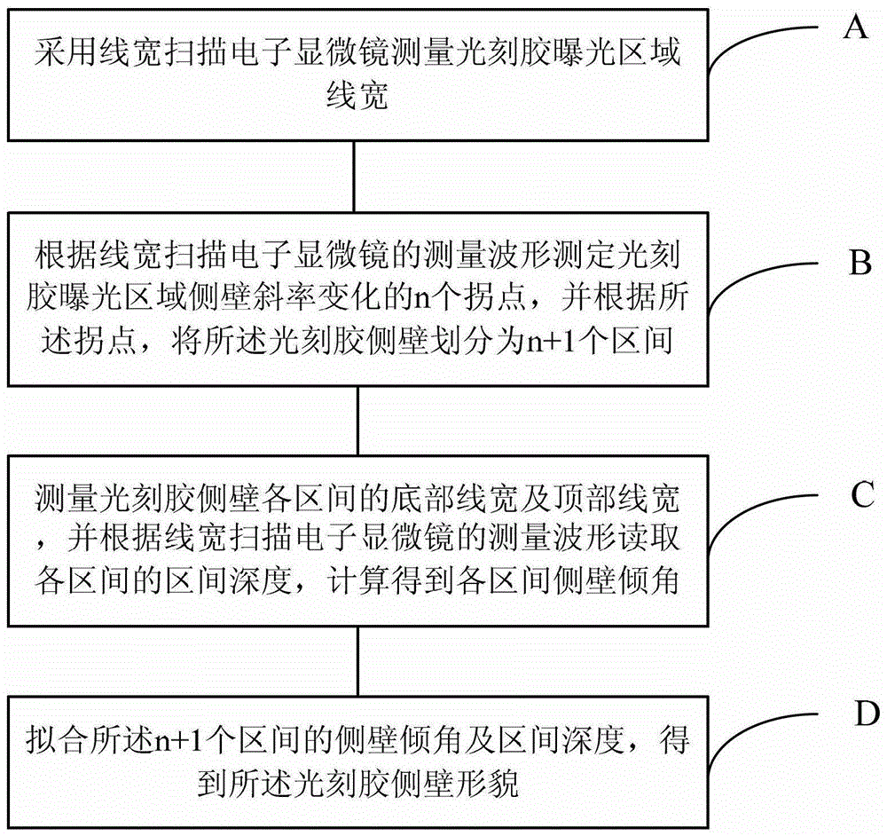
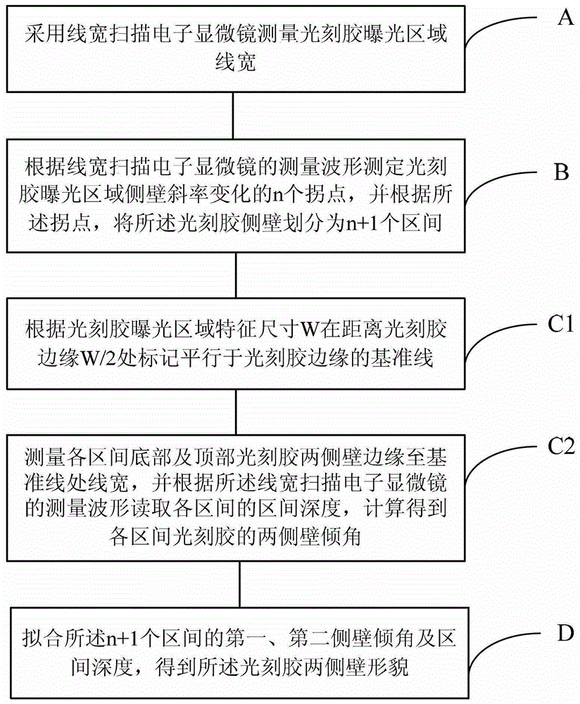
[0025] figure 1 It is a flow chart of a method for characterizing a photoresist profile provided by the first embodiment of the present invention.

[0026] Such as figure 1 As shown, the photoresist topography characterization method provided in the first specific embodiment includes the following steps:
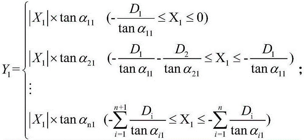
[0027] Step ...


PUM

PropertyMeasurementUnit
widthaaaaaaaaaa
widthaaaaaaaaaa

Abstract

The invention relates to the field of semiconductor manufacture, and discloses a morphology characterization method for photoresist. Inflection points of changes in the sidewall slope of a photoresist exposure area are determined, the sidewall of the photoresist is divided into a plurality of intervals according to the inflection points, an inclination angle of the sidewall of each interval is calculated by measuring the top line width, bottom line width and interval depth of the interval, and the inclination angle of the sidewall and the interval depth of each interval are fitted to obtain the morphology of the photoresist. According to the method, required measurement is top-down overlooked line width measurement, a wafer to be measured is not required to be sliced in a characterization process, profile scanning is not required, the morphology of the sidewall of the photoresist can be accurately characterized without any unrecoverable damage, the method can be used for the capability improvement and verification of a photoresist process, and is also applicable to quality control in a production process, the photoetching quality can be further ensured, and the device integration level and the industrial yield can be effectively improved.

Description

Technical field [0001] The invention relates to the field of semiconductor manufacturing, in particular to the photoresist characterization technology after development in the photolithography process. Background technique [0002] Photolithography plays a vital role in the semiconductor manufacturing process. Its pattern resolution, overlay accuracy, photoresist sidewall morphology, photoresist defects, and photoresist resistance to etching are all directly affected Success or failure of subsequent processes. [0003] In photolithography, the process performance capability of photoresist plays an important role. However, the negative photoresist coating is less sensitive to environmental factors and has low resolution, and is not suitable for small-size, thin-line lithography. With the advancement of integrated circuit manufacturing process and the shrinking of feature size, the integration of integrated circuit chips is getting higher and higher. Can a positive photoresist incl...

Claims


Application Information

Patent Timeline
Patent Type & Authority Patents(China)
IPC IPC(8): G03F7/20
Inventor 姚树歆戴峻储佳
Owner SHANGHAI INTEGRATED CIRCUIT RES & DEV CENT
Why Eureka
Try Eureka