Separate gate type flash memory of embedded logic circuit and fabricating method thereof

A technology of separating gates and manufacturing methods, which is applied in the manufacture of circuits, electrical solid-state devices, semiconductor/solid-state devices, etc., can solve problems such as memory operating speed signal transmission bandwidth limitations, achieve increased density, reduce costs, and simplify manufacturing processes Effect

Active Publication Date: 2013-03-06
SEMICON MFG INT (SHANGHAI) CORP
View PDF4 Cites 27 Cited by
  • Summary
  • Abstract
  • Description
  • Claims
  • Application Information

AI Technical Summary

Problems solved by technology

[0005] If the split-gate flash memory, high-voltage transistors, and logic transistors are all built on a separate integrated chip, the operating speed of the entire memory will be limited by the signal transmission bandwidth between the flash memory and peripheral circuits

Method used


Image

  • Separate gate type flash memory of embedded logic circuit and fabricating method thereof
  • Separate gate type flash memory of embedded logic circuit and fabricating method thereof
  • Separate gate type flash memory of embedded logic circuit and fabricating method thereof

Examples


Embodiment Construction

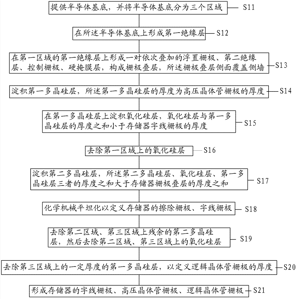
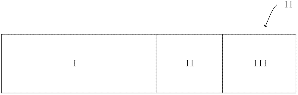
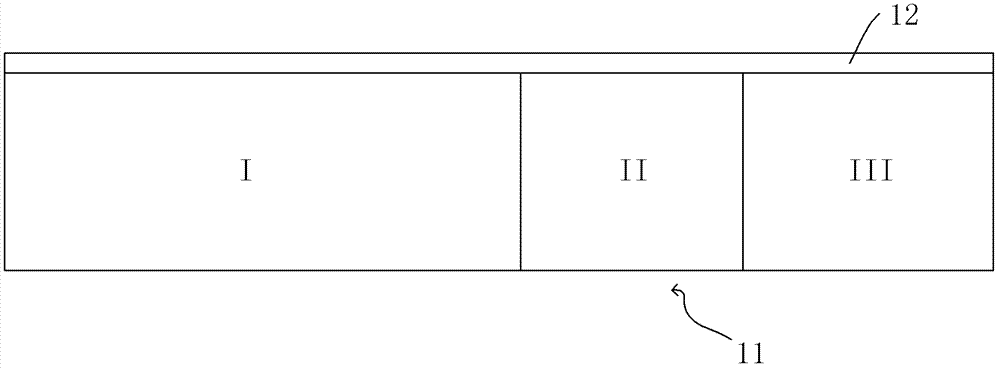
[0036] The present invention hopes to form separate gate type flash memory gates, high-voltage transistor gates, and logic transistor gates with different thicknesses on the same semiconductor substrate by the following method: provide a semiconductor substrate, and the semiconductor substrate is divided into three parts There are three areas: the first area, the second area, and the third area. A pair of floating gates, a second insulating layer, a control gate, and a hard mask layer are formed on the first region to form a gate stack; a first polysilicon layer is deposited, and the thickness of the polysilicon layer is The thickness required for the gate of the high-voltage transistor; a silicon oxide layer is deposited on the first polysilicon layer, and then the silicon oxide layer on the first region is removed, and the sum of the thicknesses of the silicon oxide layer and the first polysilicon layer is equal to the thickness of the first polysilicon layer The gate stacks...


PUM


Abstract

The invention provides a fabricating method of a separate gate type flash memory of an embedded logic circuit. Compared with a forming method of a single separate gate type flash memory, the separate gate type flash memory, a high voltage transistor and a logic transistor can be simultaneously fabricated on one integrated circuit by five techniques of primary silicon oxide deposition, primary polycrystalline silicon deposition, secondary etching and primary silicon oxide layer removal, therefore, the densities of the three elements are increased, the integration degree is high, the operation speed is faster, and the integrated chip is smaller, so that the cost of each integrated chip is reduced, and the application is more extensive. Furthermore, in the forming process of the separate gate type flash memory of embedded logic circuit, the grids of the high voltage transistor and the logic transistor have few defects to meet the quality demands of the grids. Correspondingly, the invention further provides a separate gate type flash memory of the embedded logic circuit.

Description

technical field [0001] The invention relates to the technical field of semiconductors, in particular to a split-gate flash memory embedded in a logic circuit and a manufacturing method thereof. Background technique [0002] Random access memory, such as DRAM and SRAM, has the problem of data loss after power failure during use. To overcome this problem, various nonvolatile memories have been designed and developed. Recently, flash memory based on the floating gate concept has become the most versatile non-volatile memory due to its small cell size and good performance. The non-volatile memory mainly includes two basic structures: a stack gate structure and a split gate structure. The stacked gate memory includes a tunnel oxide layer, a floating gate polysilicon layer for storing electrons, an oxide / nitride / oxide (oxide-nitride-oxide, ONO) stack layer and The control gate polysilicon layer that controls the storage and release of electrons. Split gate memory also includes...

Claims


Application Information

Patent Timeline
Patent Type & Authority Applications(China)
IPC IPC(8): H01L21/8234H01L27/04
Inventor 王友臻周儒领詹奕鹏
Owner SEMICON MFG INT (SHANGHAI) CORP
Why Eureka
Try Eureka