Compound semiconductor laminated film solar cell

A thin-film solar cell and semiconductor technology, used in semiconductor devices, circuits, photovoltaic power generation, etc., can solve the problems of requiring three or four contacts, increasing the cost of battery production, and being unable to directly connect internally. The effect of reverse junction phenomenon and solving process compatibility problems

Active Publication Date: 2013-03-06
CHINA ELECTRONIC TECH GRP CORP NO 18 RES INST
View PDF4 Cites 5 Cited by
  • Summary
  • Abstract
  • Description
  • Claims
  • Application Information

AI Technical Summary

Problems solved by technology

Currently known I-III-VI chalcopyrite compound semiconductor double-junction thin-film solar cells have realized that the top cell adopts a wide bandgap semiconductor material and a transparent conductive oxide as the back contact, which improves the conversion efficiency of the solar cell, but due to the I- The III-VI chalcopyrite compound cannot realize the tunnel junction, the process compatibility between the bottom cell and the top cell is poor, and the direct internal connection between the bottom cell and the top cell cannot be directly connected, and the external cascading method is often used. As a result, the entire cell needs three One or four contacts make the structure of the battery complex and increase the manufacturing cost of the battery

Method used


Image

  • Compound semiconductor laminated film solar cell

Examples


Embodiment Construction

[0019] In order to further disclose the invention content, features and effects of the present invention, the following examples are specifically cited and described in detail in conjunction with the accompanying drawings as follows.

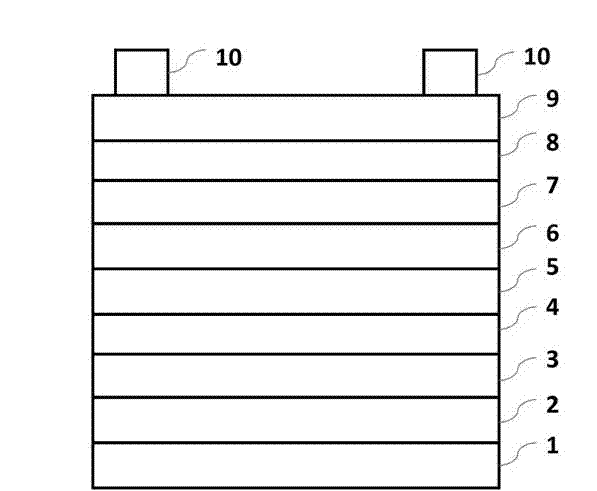
[0020] Compound semiconductor stacked thin film solar cells, including a narrow bandgap copper indium gallium selenide bottom cell and a wide band gap copper gallium selenide top cell.

[0021] Innovation point of the present invention is:

[0022] The bottom cell and the top cell are connected in series inside the connection layer; the connection layer is composed of a transparent metal oxide conductive layer located at the bottom cell and a nano-metal conductive layer located at the top cell; the transparent metal oxide conductive layer is One of the TCO films formed by 300-600nm thick Al, Ga or In-doped ZnO, or ITO film; the nano-metal conductive layer is a Mo film with a thickness of 30-50nm; the narrow bandgap copper indium gallium selenide...


PUM

PropertyMeasurementUnit
thicknessaaaaaaaaaa
conversion efficiencyaaaaaaaaaa

Abstract

The invention relates to a compound semiconductor laminated film solar cell, comprising a copper indium gallium selenide cell (CIGS) bottom cell with a low bandgap and a copper gallium selenide (CGS) top cell with a high bandgap. The compound semiconductor laminated film solar cell is characterized in that the bottom cell and the top cell are internally connected in series into a whole through a connecting layer; and the connecting layer is composed of a transparent metal oxide conductive layer positioned at the bottom cell and a nanometer metal conductive layer positioned at the top cell. According to the compound semiconductor laminated film solar cell, the combination of transparent metal oxide and a nanometer metal film is used as the connecting layer of the bottom cell and the top cell, so that the technological compatibility problem of the bottom cell and the top cell is solved, the internal electrical connection of the bottom cell and the top cell is realized, the manufacturing process of the cell is simplified, the manufacturing cost of the cell is reduced, and the cell is simple in structure.

Description

technical field [0001] The invention belongs to the technical field of thin film solar cells, in particular to a compound semiconductor stacked thin film solar cell. Background technique [0002] At present, the solar cells used in the market are still dominated by the first-generation monocrystalline silicon / polycrystalline silicon cells, but the second-generation thin-film solar cells are recognized as the main direction of solar cell development in the future. Thin-film solar cells refer to solar cells made of materials with a thickness on the order of microns, which is one of the most effective ways to greatly reduce the cost of solar cells. Among many thin-film solar cells, I-III-VI compound semiconductor copper indium (gallium) selenium thin-film solar cells (also known as Cu(In,Ga)Se 2 (referred to as CIGS thin-film solar cells) has become a research hotspot in the photovoltaic industry due to its high conversion efficiency, good long-term stability, and strong radia...

Claims


Application Information

Patent Timeline
Patent Type & Authority Applications(China)
IPC IPC(8): H01L31/0725H01L31/0749H01L31/02
CPCY02E10/50Y02E10/541Y02P70/50
Inventor 李微杨立杨盼闫礼赵彦民冯金晖乔在祥
Owner CHINA ELECTRONIC TECH GRP CORP NO 18 RES INST
Why Eureka
Try Eureka