Electro-optical modulation system and electro-optical switch or optical attenuator formed by electro-optical modulation system

An electro-optic modulation and electro-optic technology, applied in optics, instruments, circuits, etc., can solve the problem of low carrier injection efficiency and achieve the effect of improving carrier injection efficiency, reducing power consumption, and reducing overall power consumption

Inactive Publication Date: 2013-03-13
上海硅通半导体技术有限公司
View PDF7 Cites 10 Cited by
  • Summary
  • Abstract
  • Description
  • Claims
  • Application Information

AI Technical Summary

Problems solved by technology

[0007] The purpose of the present invention is to overcome the deficiencies of the prior art, provide an electro-optical modulation system and an electro-optic switch or an optical attenuator composed of it, solve the problem of low carrier injection efficiency in the prior art, and reduce the total power consumption of the device , and has a high extinction ratio

Method used


Image

  • Electro-optical modulation system and electro-optical switch or optical attenuator formed by electro-optical modulation system
  • Electro-optical modulation system and electro-optical switch or optical attenuator formed by electro-optical modulation system
  • Electro-optical modulation system and electro-optical switch or optical attenuator formed by electro-optical modulation system

Examples


Embodiment Construction

[0022] Below by specific embodiment and in conjunction with accompanying drawing, the present invention is described in detail:

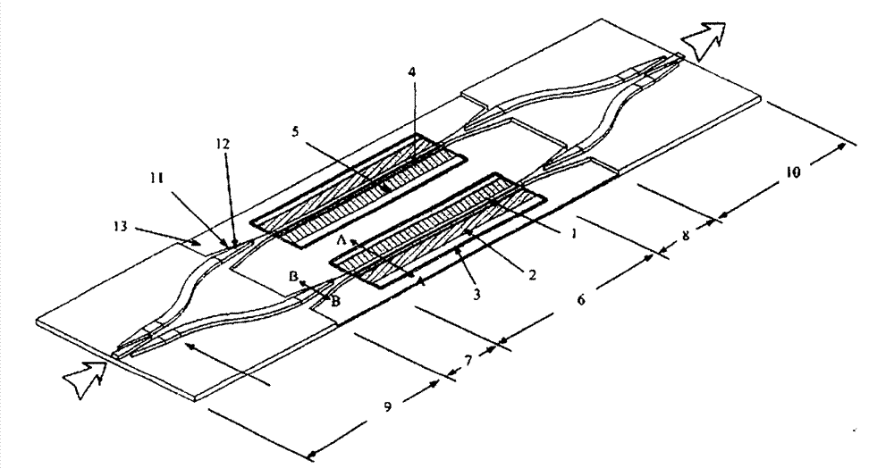
[0023] In order to solve the problems existing in the existing electro-optic PIN diode, the present invention provides an electro-optic modulation system comprising a high-injection-efficiency electro-optic PIN diode waveguide and a pair of mode converters, and a single-mode working system composed of such an electro-optic modulation system electro-optic switch or optical attenuator.

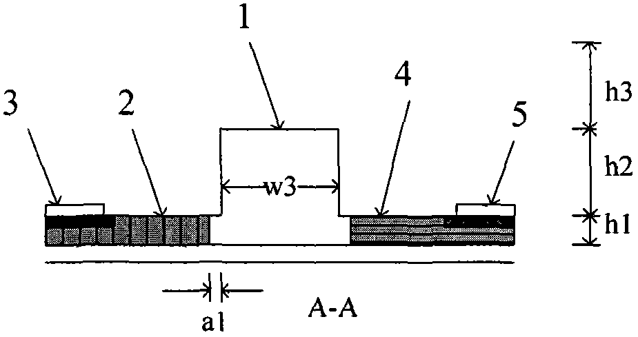
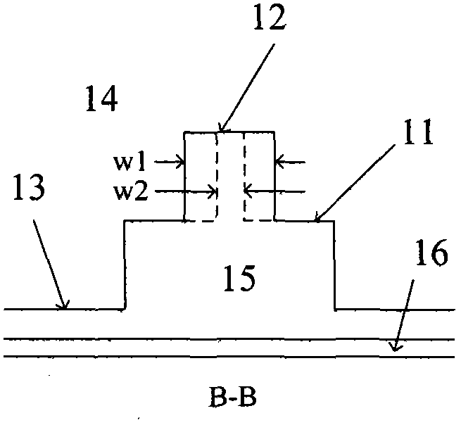
[0024] figure 1 A schematic diagram of an electro-optic switch or an optical attenuator constituted by the electro-optic modulation system disclosed in the present invention is given. The electro-optical switch or optical attenuator is a waveguide device of semiconductor material. The main light-guiding layer of a waveguide is a semiconductor material, such as silicon. Such as figure 1 As shown, the electro-optical switch or optical attenuation includes an input Y...


PUM


Abstract

The invention discloses an electro-optical modulation system and an electro-optical switch or optical attenuator formed by the electro-optical modulation system. The electro-optical modulation system comprises an electro-optical PIN diode waveguide and a pair of mode convertors, wherein the electro-optical PIN diode waveguide is composed of a ridge waveguide; a high-concentration doped P-type doping area and an N-type doping area are respectively arranged on the two sides of a flat area of the ridge waveguide; the height of the flat area of the ridge waveguide is less than a half of the ridge height of the ridge waveguide; the ridge width of the ridge waveguide is close to the total height of the ridge waveguide; and the main energy of a main mould for waveguide conduction is limited in a core area. The electro-optical switch or optical attenuator comprises an input Y branch coupler, a pair of input mode convertors, a section of active waveguide area, a pair of output mode convertors, and an output Y branch coupler in turn from input to output, wherein the active waveguide area is composed of two parallel electro-optical PIN diode waveguides. The structure of the electro-optical modulation system can increase the charge-carrier injection efficiency, can reduce total power consumption of devices and has high extinction ratio.

Description

technical field [0001] The invention relates to an integrated optoelectronic device, in particular to an electro-optic modulation system and an electro-optic switch or an optical attenuator composed of it. Background technique [0002] In PIN diodes based on charge injection, modulating the concentration of free carriers in the intrinsic region of PIN diodes will cause changes in the refractive index and absorption coefficient (imaginary part of the refractive index) of semiconductor materials. [0003] At present, there are already many documents and patents on silicon-based electro-optic modulators and electro-optic switches based on the above structure. The biggest problem with this technology is that the charge injection efficiency is too low. Especially when the PIN diode is driven by a forward voltage, the injection of many sub-holes in the P-type doped region and many sub-electrons in the N-type doped region to the intrinsic region is affected by the doping of the P-...

Claims


Application Information

Patent Timeline
Patent Type & Authority Applications(China)
IPC IPC(8): G02F1/015H01L33/00H01L33/20
Inventor 李冰
Owner 上海硅通半导体技术有限公司
Why Eureka
Try Eureka