Preparation method of back passivated crystalline silicon solar cell

A solar cell and backside passivation technology, which is applied in the direction of circuits, electrical components, semiconductor devices, etc., can solve the problems that are not suitable for large-scale production, silicon wafers are easily polluted, and the process flow is too many, so as to improve the conversion efficiency of cells and save energy. Process time, avoid process effect

Inactive Publication Date: 2013-03-13
NINGBO ULICA SOLAR SCIENCE & TECHNOLOGY CO LTD
View PDF4 Cites 7 Cited by
  • Summary
  • Abstract
  • Description
  • Claims
  • Application Information

AI Technical Summary

Problems solved by technology

However, this type of method has many procedures, poor repeatability, and silicon wafers are easily contaminated, so it is not suitable for large-scale production.

Method used


Image

  • Preparation method of back passivated crystalline silicon solar cell
  • Preparation method of back passivated crystalline silicon solar cell
  • Preparation method of back passivated crystalline silicon solar cell

Examples


preparation example Construction

[0020] A method for preparing a backside passivated crystalline silicon solar cell, comprising the following steps:

[0021] (1) Process the graphite baffle in the graphite boat to form a hollowed-out mesh structure;

[0022] (2) Put the silicon wafer in the silicon wafer flower basket and wait for coating after texturing, diffusion to make PN junction, peripheral etching, and removal of phospho-silicate glass; the steps described in this step are all existing technologies, and will not be expanded here in detail .

[0023] (3) Put the silicon wafer processed in step (2) into the graphite boat processed in step (1), so that the back of the silicon wafer is close to the graphite baffle, and use the coating equipment to cover the unobstructed area and the front of the silicon wafer At the same time, a silicon nitride film is deposited. The coating equipment is also called PECVD equipment.

[0024] (4) Screen-print the back electrode, back electric field and front electrode on...

specific Embodiment 1

[0026] Specific embodiment one: a kind of preparation method of rear passivation crystalline silicon solar cell, comprises the following steps:

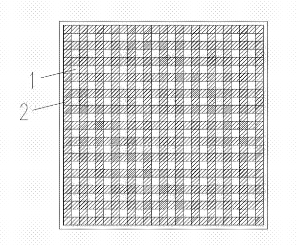
[0027] (1) Process the graphite baffle in the graphite boat to form a figure 1 In the network structure shown, the hollow part is a square with a side length of 6mm, and a total of 144 squares are evenly arranged on the graphite baffle. Then put the graphite baffle into the graphite boat and fix it;

[0028] (2) After the silicon wafer is textured, diffused to make a PN junction, the periphery is etched, and the phospho-silicate glass is removed, it is placed in a silicon wafer flower basket and waits for coating;

[0029] (3) Put the silicon wafer processed in step (2) in the graphite boat, so that the back of the silicon wafer is close to the graphite baffle, and use PECVD equipment to coat the silicon nitride film on the front and back of the silicon wafer at the same time;

[0030] (4) Screen-print the back electrode, back elec...

specific Embodiment 2

[0031] Specific embodiment two: a kind of preparation method of rear passivation crystalline silicon solar cell, comprises the following steps:

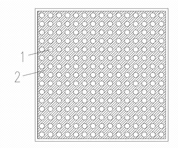
[0032] (1) Process the graphite baffle in the graphite boat to form a figure 2 In the network structure shown, the hollow part is a circle with a diameter of 6 mm, and a total of 225 circles are evenly arranged on the graphite baffle. Then put the graphite baffle into the graphite boat and fix it;

[0033] (2) After the silicon wafer is textured, diffused to make a PN junction, the periphery is etched, and the phospho-silicate glass is removed, it is placed in a silicon wafer flower basket and waits for coating;

[0034] (3) Put the silicon wafer processed in step (2) in the graphite boat, so that the back of the silicon wafer is close to the graphite baffle, and use PECVD equipment to coat the silicon nitride film on the front and back of the silicon wafer at the same time;

[0035] (4) Screen-print the back electrode, the back e...


PUM


Abstract

The invention relates to the field of preparation of a crystalline silicon solar cell, in particular to a preparation method of the back passivated crystalline silicon solar cell. The method comprises the steps of: (1) machining a graphite baffle in a graphite boat to form a hollowed net structure; (2) making herbs into wool, diffusing to make a PN knot, etching peripherally, removing phosphorosilicate glass for a silicon wafer and packaging the silicon wafer in a silicon wafer basket to be coated; (3) packaging the silicon wafer processed by the step (2) in the graphite coat processed in the step (1), so that the silicon is attached to the graphite baffle on the back; and plating silicon nitride thin films on a barrier-free area on the back and front surfaces of the silicon wafer by using a film coating device; and (4) screen printing a back electrode, a back electric field and a front electrode on the silicon wafer coated on both sides; and then co-sintering to prepare the back passivated crystalline silicon solar cell. The method provided by the invention is low in cost and good in repeatability, and is suitable for industrialized production in batches.

Description

technical field [0001] The invention relates to the field of preparation of crystalline silicon solar cells, in particular to a method for preparing back passivated crystalline silicon solar cells. Background technique [0002] The preparation process of traditional crystalline silicon solar cells is as follows: silicon wafer texturing; diffusion to make PN junction; peripheral etching; removal of phospho-silicate glass; deposition of silicon nitride film on the front side by coating equipment; Electric field and front electrode; co-sintering to complete the entire battery preparation process. The coating equipment is based on plasma enhanced chemical vapor deposition (PECVD). [0003] The development direction of crystalline silicon solar cells is low cost and high efficiency. In terms of improving efficiency, it is currently more effective to coat the back of the solar cell with a film with good passivation effect, such as silicon dioxide film, silicon nitride film, alum...

Claims


Application Information

Patent Timeline
Patent Type & Authority Applications(China)
IPC IPC(8): H01L31/18
CPCY02P70/50
Inventor 蔡二辉刘伟余涛陈筑刘晓巍
Owner NINGBO ULICA SOLAR SCIENCE & TECHNOLOGY CO LTD
Why Eureka
Try Eureka