Electrolytic copper-clad plate by taking polymethyl methacrylate as medium, printed circuit board and manufacturing method thereof

A printed circuit board and manufacturing method technology, which is applied in the secondary processing of printed circuits, chemical instruments and methods, improvement of metal adhesion of insulating substrates, etc. Problems such as poor ability, to achieve the effect of less difficulty in processing, good insulation and mechanical strength, and low cost

Inactive Publication Date: 2013-03-20
SHENZHEN WUZHU TECH
View PDF4 Cites 3 Cited by
  • Summary
  • Abstract
  • Description
  • Claims
  • Application Information

AI Technical Summary

Problems solved by technology

[0003] In the prior art, epoxy resin as the main body (FR-4) is currently the largest and most widely used type of product for printed circuit boards. However, printed circuit boards made of FR-4 materials have high cost and large dielectric loss. And the electrical performance is poor, and FR-4 has a series of shortcomings such as easy water absorption, easy aging, and poor voltage resistance, which makes the printed circuit boards made of it not suitable for special environments, especially humid environments, aerospace, high-speed, etc. Communications, space or radioactive medical devices) and other fields require materials with light density, low transmission dielectric loss, strong corrosion resistance, environmental protection, and high insulation.

Method used


Image

  • Electrolytic copper-clad plate by taking polymethyl methacrylate as medium, printed circuit board and manufacturing method thereof
  • Electrolytic copper-clad plate by taking polymethyl methacrylate as medium, printed circuit board and manufacturing method thereof
  • Electrolytic copper-clad plate by taking polymethyl methacrylate as medium, printed circuit board and manufacturing method thereof

Examples


Embodiment Construction

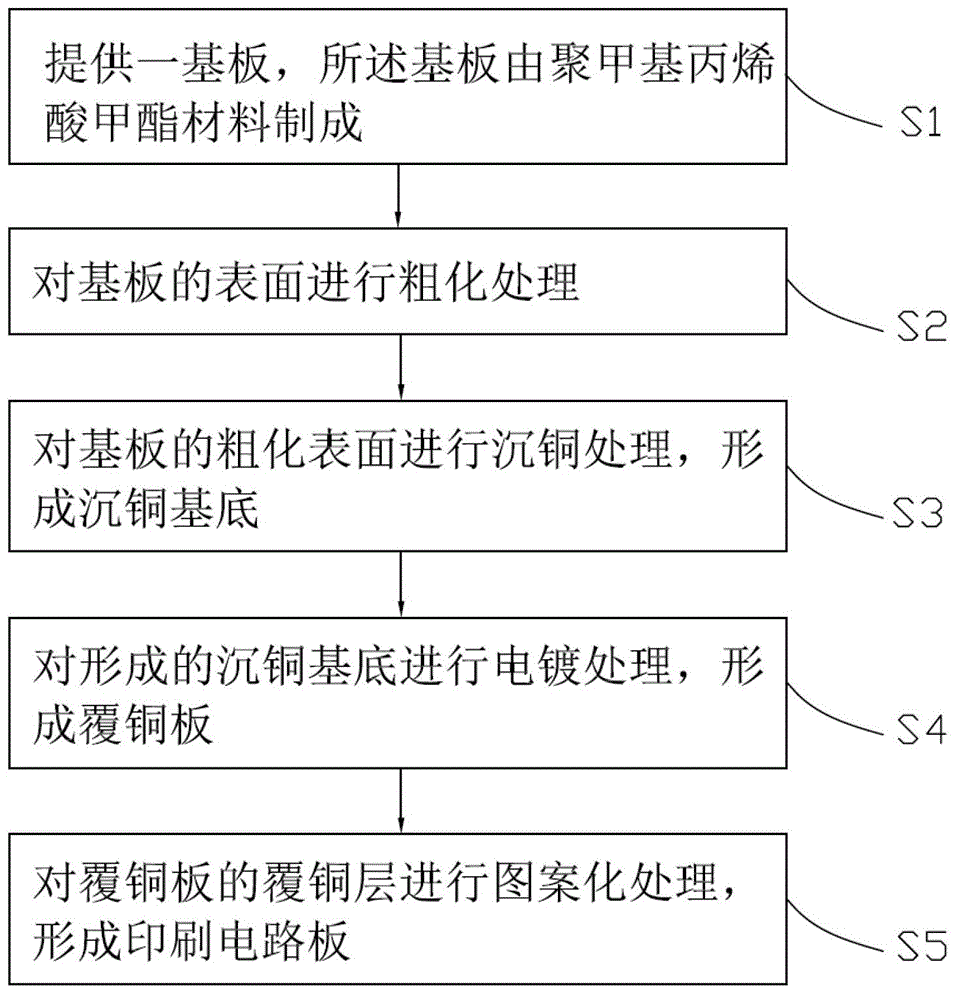
[0030] Specific embodiments of the present invention will be described in detail below in conjunction with the accompanying drawings.

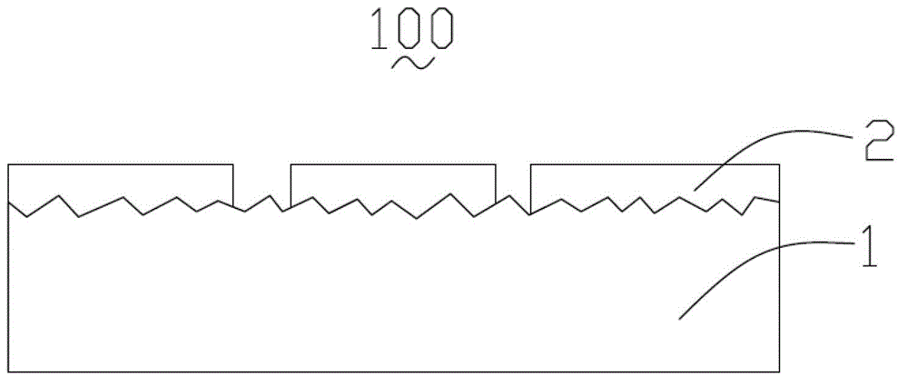
[0031] see figure 1 , figure 1 It is a schematic cross-sectional structure diagram of a printed circuit board (Printed Circuit Board, PCB) of the present invention. The printed circuit board 100 includes a substrate 1 and a patterned copper layer 2 disposed on the substrate 1 .

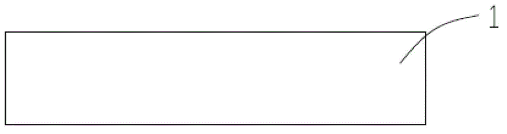
[0032] Specifically, the substrate 1 is made of polymethyl methacrylate (Polymethyl Methacrylate, PMMA) material, and its surface is roughened to form a roughness of 50 microns to 150 microns, which is beneficial to the patterned metal layer. 2. It is tightly combined with it to prevent the metal layer from falling off and warping.

[0033] The patterned copper layer 2 can also be replaced by a common conductive material such as an aluminum layer, a silver layer, or a gold layer according to actual needs, which is not specifically limited here. The patterned coppe...


PUM

PropertyMeasurementUnit
surface roughnessaaaaaaaaaa
thicknessaaaaaaaaaa

Abstract

The invention relates to a method for manufacturing a copper-clad plate. The method comprises the following steps of: providing a substrate; manufacturing a polymethyl methacrylate material, and roughening the surface of the polymethyl methacrylate material; performing electroless plating copper treatment on the roughened surface of the polymethyl methacrylate material, and forming an electroless plating copper substrate; electroplating the formed electroless plating copper substrate, and forming the copper-clad plate. The invention also provides a method for manufacturing a circuit board on the basis of the method for manufacturing the copper-clad plate. The invention further provides a copper-clad plate and a printed circuit board. The printed circuit board has the advantages of excellent electrical properties and mechanical properties, wide application range and low cost.

Description

technical field [0001] The invention relates to a copper-clad laminate, a printed circuit board and a manufacturing method thereof, in particular to a copper-clad laminate, a printed circuit board and a manufacturing method thereof with PMMA (polymethyl methacrylate) material as a substrate. Background technique [0002] Printed Circuit Board (PCB) is the basis of almost any electronic product. With the rapid development of the electronics industry, printed circuit boards, as the basic components of electronic products, are more and more widely used. Although the functions of electronic products are not only enhanced, the application With the expansion of the field, especially driven by the development of the high-speed information age, there are more and more requirements for printed circuit boards used in electronic products, especially the requirements for printed circuit boards in terms of signal transmission quality and speed. constantly improving. [0003] In the prio...

Claims


Application Information

Patent Timeline
Patent Type & Authority Applications(China)
IPC IPC(8): B32B15/09B32B38/18H05K3/38
Inventor 徐学军曾志蔡志浩李春明
Owner SHENZHEN WUZHU TECH
Why Eureka
Try Eureka