Fe-Si-Al ternary amorphous thin film with adjustable band gap width and preparation method of thin film

A fe-si-al, amorphous thin film technology, applied in the direction of ion implantation plating, coating, metal material coating process, etc., can solve multi-phase hybrid deterioration, large film base mismatch, prone to stacking faults, Twins and other problems can be avoided to avoid multi-phase mixing, avoid lattice mismatch, and ensure the effect of composition and performance

Inactive Publication Date: 2013-04-03
DALIAN UNIV OF TECH
View PDF6 Cites 4 Cited by
  • Summary
  • Abstract
  • Description
  • Claims
  • Application Information

AI Technical Summary

Problems solved by technology

The crystals are also prone to defects such as stacking faults and twins, so it is difficult to obtain high-quality and pure β-FeSi 2 Material
[0004] (2) β-FeSi 2 When used in the field of optoelectronics, most of the thin films are prepared on the basis of single crystal Si, but there is a large film-base mismatch problem, resulting in many of its properties failing to meet theoretical expectations.
[0005] (3) Binary β-FeSi currently prepared using different methods 2 material, whose bandgap width varies around 0.87eV, is slightly different, but cannot be modulated
Crystalline ternary FeSi after adding the third component 2 Type materials are prone to phase separation. Although the bandgap width can be modulated in a wide range, it increases the instability of the structure and further deteriorates the situation of multiphase mixing.

Method used


Image

  • Fe-Si-Al ternary amorphous thin film with adjustable band gap width and preparation method of thin film
  • Fe-Si-Al ternary amorphous thin film with adjustable band gap width and preparation method of thin film
  • Fe-Si-Al ternary amorphous thin film with adjustable band gap width and preparation method of thin film

Examples


Embodiment 1

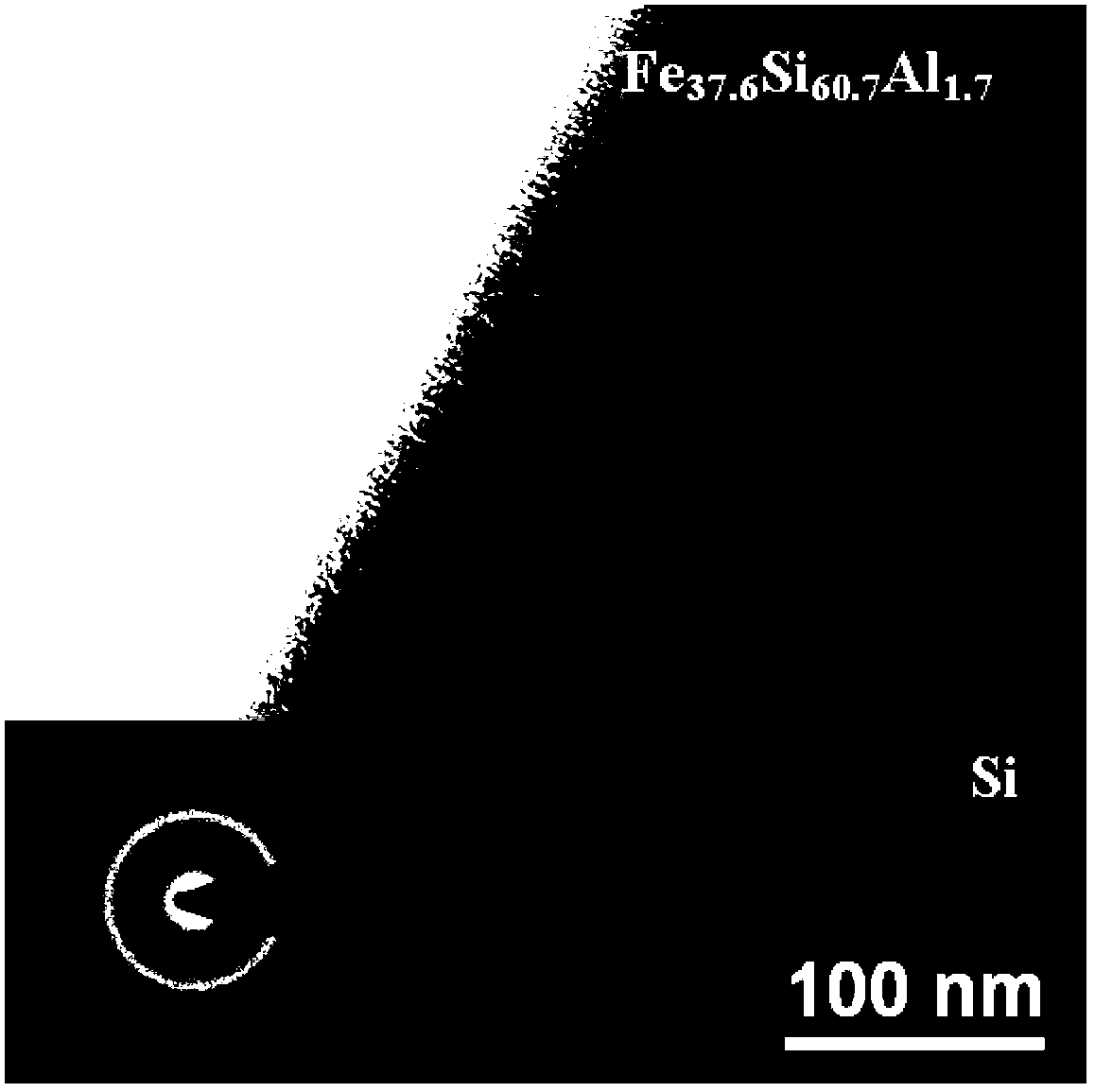
[0031] Embodiment 1: Fe is prepared by magnetron sputtering method 37.6 Si 60.7 al 1.7 film

[0032] (1) Preparation of alloy sputtering target, the steps are as follows:

[0033] 1. material preparation: according to the atomic percentage of Fe and Al being 4:0.15 to take each component value, the purity of Fe and Al metal raw materials to be used: Fe is 99.99%, and Al is 99.999%;

[0034] ② Fe 4 al 0.15 Melting of alloy ingots: Put the metal mixture in the water-cooled copper crucible of the melting furnace, and use the method of vacuum arc melting to melt under the protection of argon. First, vacuumize to 10 -2 Pa, then filled with argon until the pressure is 0.03±0.01MPa, the control range of melting current density is 150±10A / cm 2 After melting, continue to smelt for 10 seconds, turn off the power, let the alloy cool down to room temperature with the copper crucible, then turn it over, put it back in the water-cooled copper crucible, and carry out the second smeltin...

Embodiment 2

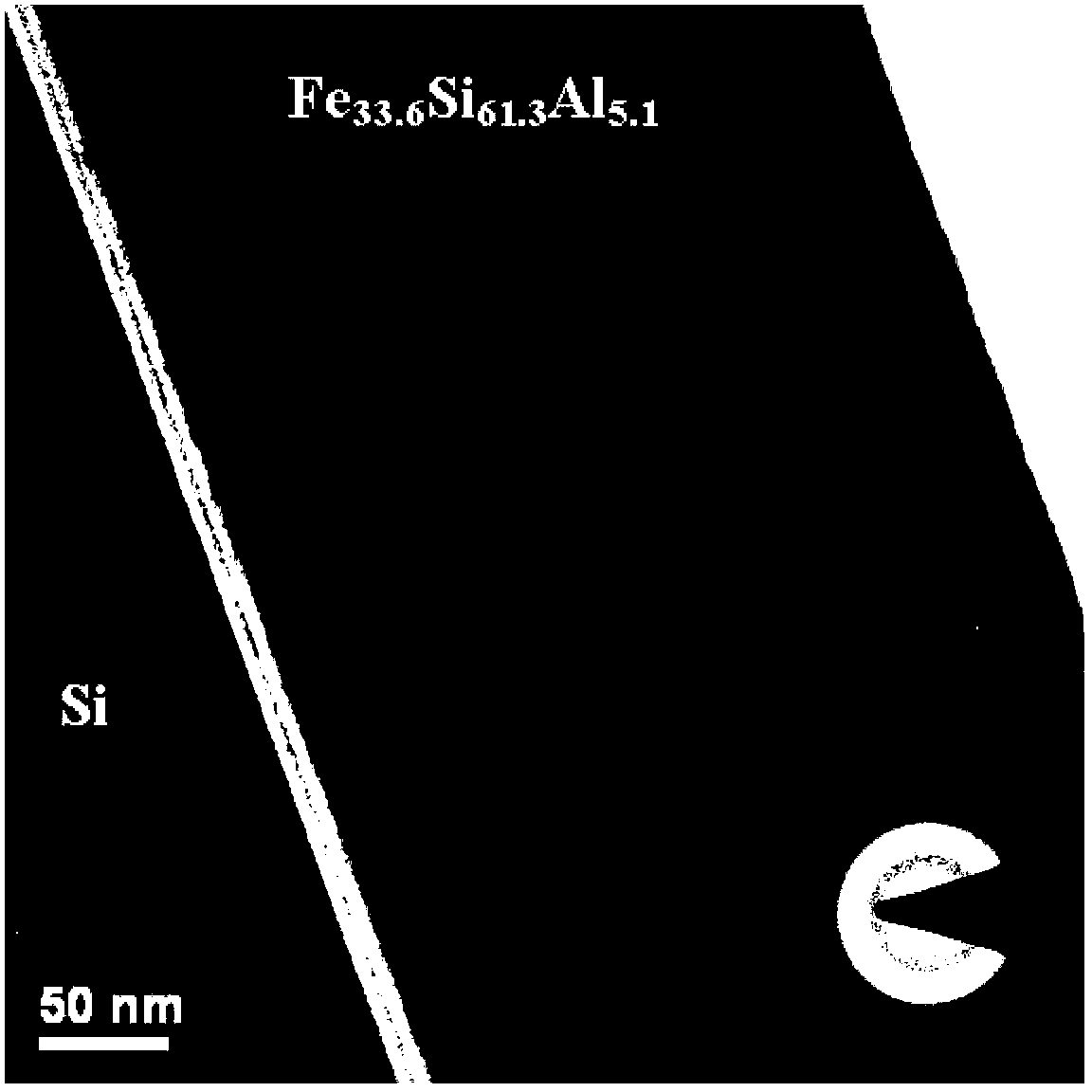
[0045] Embodiment 2: Fe is prepared by magnetron sputtering method 33.6 Si 61.3 al 5.1 film

[0046] The preparation process is the same as in Example 1, only the Fe of the combined alloy sputtering target is adjusted. 4 al z Number of alloy sheets and Z value: from 5.5 sheets of Fe 4 al 0.5 The alloy sheet is pasted on the basic Si target used for sputtering. According to EPMA analysis, the contents of Fe, Si and Al in the film are 33.6at.%, 61.3at.%, and 5.1at.%. The XRD and TEM results showed that the Fe 33.6 Si 61.3 al 5.1 No crystal information was found in the sample, indicating that the prepared amorphous film was prepared. The bandgap width was measured to be 0.60eV.

Embodiment 3

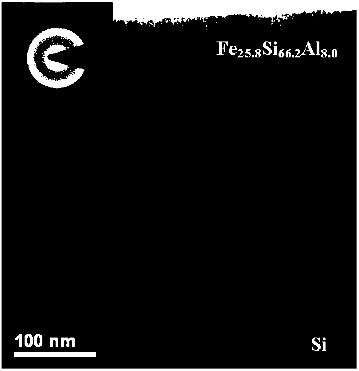
[0047] Embodiment 3: Fe is prepared by magnetron sputtering method 25.8 Si 66.2 al 8.0 film

[0048] The preparation process is the same as in Example 1, only the Fe of the combined alloy sputtering target is adjusted. 4 al z Number of alloy sheets and Z value: 4 sheets of Fe 4 al 1 The alloy sheet is pasted on the basic Si target used for sputtering. According to EPMA analysis, the contents of Fe, Si, and Al in the film are 25.8 at.%, 66.2 at.%, and 8.0 at.%. The XRD and TEM results showed that the Fe 25.8 Si 66.2 al 8.0 No crystal information was found in the sample, indicating that the prepared amorphous film was prepared. The bandgap width was measured to be 0.50eV.


PUM

PropertyMeasurementUnit
thicknessaaaaaaaaaa

Abstract

The invention discloses a Fe-Si-Al ternary amorphous thin film with adjustable band gap width and a preparation method of the thin film, belonging to the technical field of semiconductor materials. The thin film comprises the following formula: Fe(1-x-y)SixAly, wherein x is not lower than 50at.% and not higher than 70at.%; y is not lower than 1at.% and not higher than 11at.%; when the total amount of (x+y) is changed to 75at.% from 60at.%, the band gap width of the thin film can be adjusted to 0.65eV from 0.45eV; and the structure of the thin film is an amorphous structure. The film has the following advantages that (1), the Fe(1-x-y)SixAly thin film is a ternary amorphous thin film with adjustable band gap width from 0.45 eV to 0.65eV; Al not only affects the band gap width, but also increases the amorphous forming ability by increasing a component element film; (2), the total amount of (Si+Al) in the film can be conveniently adjusted by changing the quantity of Fe4Alz alloy sheets and the z value in a combined sputtering target to obtain different band gap widths; (3), the thin film is kept amorphous, so that the uniformity of the components and performances can be ensured, and the problems such as lattice mismatch, and multi-phase mixing and the like in the amorphous thin film preparation are effectively avoided. The Fe-Si-Al ternary amorphous thin film with adjustable band gap width provided by the invention is suitable for manufacturing narrow band-gap semiconductor apparatuses such as an infrared detector.

Description

technical field [0001] The invention relates to a Fe-Si-Al ternary amorphous film capable of modulating the bandgap width and a preparation method thereof, belonging to the technical field of semiconductor materials. Background technique [0002] Semiconductor metal silicides are one of the materials used in solar cells. They have excellent compatibility with single crystal silicon technology, and have metal conductivity, high thermal stability, oxidation resistance and superior mechanical stability. At the same time, semiconductor Silicides have also drawn great interest for their superior environmental friendliness, especially transition metal silicides β-FeSi 2 , its raw materials Fe and Si are both rich in reserves and non-toxic and side effects, and can synthesize various safer devices. More importantly, β-FeSi 2 With a direct band gap of 0.83~0.87eV, it has a large optical absorption coefficient for infrared wavelengths (α > 10 -5 cm -1 ,1.0eV), the theoretical ...

Claims


Application Information

Patent Timeline
Patent Type & Authority Applications(China)
IPC IPC(8): C23C14/14C23C14/35
Inventor 李晓娜郑月红董闯
Owner DALIAN UNIV OF TECH
Why Eureka
Try Eureka